Views: 0 Author: Site Editor Publish Time: 2025-04-10 Origin: Site


Thinking and solving the gate problem of SIC MOS tube
As a new type of power semiconductor device, SIC MOS tube has been widely used in new energy vehicles, photovoltaics, smart grids and other fields in recent years with the maturity of technology. It has significant advantages such as fast switching speed, low on-resistance and high temperature resistance, and has gradually become a powerful substitute for traditional silicon-based devices.
Taking new energy vehicles as an example, SIC MOS tubes are used in on-board inverters to improve power conversion efficiency, reduce energy loss, and thus increase the vehicle's cruising range. In the photovoltaic field, photovoltaic inverters using SIC MOS tubes can achieve higher power density and conversion efficiency, reducing system costs.
The importance of studying the gate problem
As the key control end of the SIC MOS tube, its performance and reliability directly affect the working stability and life of the entire device. Once the gate is damaged, the SIC MOS tube will not work properly, resulting in failure of the entire circuit system; As a new type of power semiconductor device, SIC MOS tube has been widely used in new energy vehicles, photovoltaics, smart grids and other fields with the maturity of technology in recent years. It has significant advantages such as fast switching speed, low on-resistance, and high temperature resistance, and has gradually become a powerful substitute for traditional silicon-based devices.

Overview of chip process structure
The chip process structure of SIC MOS tube mainly includes substrate, epitaxial layer, source, drain, gate and insulating layer. Among them, the substrate is usually made of silicon carbide material, which has the characteristics of high thermal conductivity and high breakdown electric field strength, providing good physical support and electrical foundation for the device. The epitaxial layer grows on the substrate and is used to accurately control the electrical parameters of the device.
The source and drain are located on both sides of the chip, which are the input and output ends of the current. The gate is separated from the channel by an insulating layer. The conduction and cutoff of the channel are controlled by applying voltage, thereby realizing the regulation of current. The insulating layer is usually made of materials such as silicon dioxide, and its quality and thickness have an important influence on the performance of the gate.
|
|
The position and function of the gate in the chip
Position: The gate is located between the source and the drain, and is closely adjacent to the channel through the insulating layer. Its main function is to control the conductivity of the channel through the electric field effect, and to achieve precise control of the conduction and shutdown of the SIC MOS tube. When a positive voltage is applied to the gate, electrons are induced in the channel to form a conductive channel, which turns on the SIC MOS tube; when the gate voltage is zero, the electrons in the channel disappear, the conductive channel is closed, and the SIC MOS tube is turned off.
Function: The control function of the gate is like the switch of a faucet, which can accurately adjust the size and on-off of the water flow (current), ensuring that the SIC MOS tube works stably and reliably in various circuit applications.

Analysis of the reasons why the gate is easily damaged
The mechanism of action of Miller capacitor
Due to factors such as polysilicon width, channel and trench width, G-pole oxide layer thickness, PN junction doping profile, SIC MOS tubes will generate parasitic capacitance, among which the key Miller capacitor Cgd plays an important role. Cgd is not constant, it will change rapidly with the change of the voltage between the gate and the drain
When the high-side MOS tube is suddenly turned on, the drain voltage of the low-side MOS tube will increase instantly. At this time, a current with a size of Miller capacitance multiplied by the voltage change rate will be generated on the Miller capacitor of the low-side MOS tube. If the gate is open, this current can only charge the Cgs capacitor below, which will cause the gate voltage to rise suddenly. When the gate voltage exceeds the gate line voltage VTH of the MOS tube, the MOS tube is prone to mis-conduction, and long-term mis-conduction will damage the gate.
Examples of problems caused by parasitic capacitance
In a half-bridge circuit, when one MOS tube is turned on, due to the existence of Miller capacitance, it will affect the gate of another MOS tube. For example, in a switching power supply application, due to the effect of Miller capacitance, the gate voltage rises abnormally, exceeding the gate voltage range, and eventually causing gate breakdown and damage, making the entire switching power supply unable to work normally.
Sources of overvoltage in external circuits
Overvoltage in external circuits may be caused by a variety of reasons, such as lightning strikes, power grid fluctuations, switching operations of inductive loads, etc. Lightning strikes can generate instantaneous high-voltage pulses, which may be transmitted to the SIC MOS tube through the power line or signal line.
When the power grid fluctuates, the sudden increase in voltage will also pose a threat to the SIC MOS tube.
When the inductive load (such as motors, transformers, etc.) is suddenly disconnected, a back electromotive force will be generated, forming a very high voltage spike. These overvoltages may be transmitted to the gate of the SIC MOS tube through the circuit, causing damage to it.
Principle of damage to the gate by overvoltage
When the voltage on the gate exceeds its rated withstand voltage, the gate oxide will break down, resulting in a decrease in the insulation performance between the gate and the channel, or even a short circuit; this will cause the gate to lose its control over the channel, and the SIC MOS tube will not work properly. In severe cases, it will cause permanent damage to the device
Overvoltage may also cause thermal effects inside the gate, causing the temperature of the gate material to rise sharply, causing the performance of the material to deteriorate, and further exacerbating the damage to the gate
Operating temperature characteristics of SIC MOS tubes
Although SIC MOS tubes have good high-temperature performance, their performance parameters will still change in high-temperature environments. As the temperature rises, the on-resistance of the SIC MOS tube will increase, the switching speed will decrease, and the leakage current will increase. Changes in these parameters will increase the power consumption of the device, generate more heat, and further aggravate the temperature rise.
When the temperature exceeds a certain limit, it will affect the material and structure of the gate, reducing the reliability of the gate
The impact of high temperature on the gate material and structure
High temperature will reduce the performance of the gate's insulating material, resulting in a decrease in the insulation resistance between the gate and the channel, increasing the risk of leakage. High temperature may also cause thermal expansion of the gate metal material, causing the connection between the gate and other components to loosen or break, affecting the normal operation of the gate.
In some high-temperature application scenarios, such as electronic equipment in the engine compartment of a car, the SIC MOS tube is in a high-temperature environment for a long time, and the probability of damage to the gate is significantly increased.
Manufacturing process defects
Common manufacturing process problems
During the manufacturing process of SIC MOS tubes, some process defects may occur, such as pinholes in the gate oxide layer, impurity contamination, photolithography deviation, etc.; these defects will cause uneven thickness of the gate oxide layer and excessive local electric field strength, thereby reducing the gate's withstand voltage capability.
Impurity contamination may change the electrical properties of the gate material and affect the normal operation of the gate. Photolithography deviation may cause insufficient dimensional accuracy of the gate, affecting the performance consistency of the device.
How process defects cause gate damage
Pinholes in the gate oxide layer will become leakage channels for current. When current passes through the pinholes, local heating will be generated, causing further damage to the oxide layer.
Impurity contamination will change the resistivity of the gate material, affect the electric field distribution of the gate, and increase the risk of gate breakdown.
The inconsistent gate size caused by photolithography deviation will cause differences in gate performance of different devices. In practical applications, gates with poor performance are more susceptible to damage.

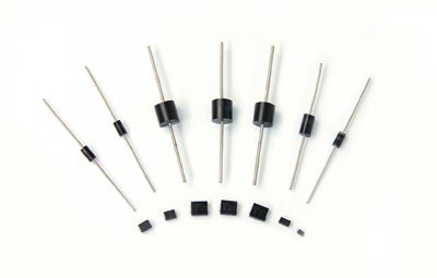
Introduction to basic working principle
SMBJ1505CA is a highly efficient circuit protection device, and its working principle is based on the avalanche breakdown effect of the PN junction. When the voltage across the TVS exceeds its breakdown voltage, the TVS will quickly turn on and clamp the overvoltage at a lower level, thereby protecting the protected device from the impact of excessive voltage. In the circuit, the TVS is usually connected in parallel with the gate of the protected SIC MOS tube. When a transient overvoltage occurs, the TVS will respond in a very short time (usually nanoseconds) and bypass the overvoltage to the ground, so that the gate voltage remains within a safe range.
SMBJ1505CA transient suppression diode is specially designed for SIC MOS tube gate protection. Its forward breakdown voltage is usually set to about 15V and the reverse breakdown voltage is set to about -5V. Such a voltage setting can match the gate operating voltage range of the SIC MOS tube, effectively protecting the gate from damage by forward and reverse overvoltages. This diode has the characteristics of fast response time, low dynamic resistance and high pulse power tolerance. The fast response time can ensure timely action at the moment of overvoltage, the low dynamic resistance can make the clamping voltage as close to the breakdown voltage as possible, and the high pulse power tolerance ensures that the diode will not be damaged when subjected to large current pulses
Reasons for using SMBJ1505CA
Prevent gate voltage fluctuations caused by crosstalk
In applications such as half-bridge circuits, the switching action of the SIC MOS tube module will cause the gate-source voltage fluctuation of the switch of another module, that is, the crosstalk problem. Positive crosstalk may cause the gate voltage to rise positively, and if it exceeds the threshold, it will cause false opening; negative crosstalk may increase the gate voltage negatively, and exceeding the negative voltage tolerance limit will cause gate breakdown. The SMBJ1505CA transient suppression diode can effectively suppress the gate voltage fluctuation caused by crosstalk. When the gate voltage rises or falls abnormally, the TVS will quickly turn on and clamp the voltage within a safe range to prevent false opening and gate breakdown.
Dealing with the threat of transient overvoltage
As mentioned above, there are various transient overvoltage threats in the external circuit, such as overvoltages generated by lightning strikes, power grid fluctuations, and inductive load switches. These overvoltages may instantly exceed the withstand voltage of the SIC MOS tube gate, causing irreversible damage to the gate.
Transient suppression diodes can respond quickly at the moment of overvoltage, limit the overvoltage within a safe range, provide reliable protection for the gate of SIC MOS tubes, and ensure that the device works normally in harsh electrical environments.
Benefits of adding transient suppression diodes
By suppressing overvoltage and crosstalk, transient suppression diodes can effectively reduce the electrical stress on the gate and reduce the risk of gate damage, thereby improving the reliability and stability of the gate of SIC MOS tubes. This helps to extend the service life of SIC MOS tubes, reduce the occurrence of equipment failures, and improve the reliability of the entire circuit system.
In the fields of industrial automation, power electronics, etc., the reliability and stability of equipment are crucial. Using transient suppression diodes to protect the gate can ensure long-term stable operation of the equipment and reduce maintenance costs.