Views: 0 Author: Site Editor Publish Time: 2024-06-11 Origin: Site


Although silicon technology and the industrial chain are mature, and the chip manufacturing cost is low, the physical properties of the material limit its application in optoelectronics, high-frequency and high-power devices, and high-temperature devices. The three generations of semiconductor materials have different characteristics, which also determines their own advantages and is suitable for different application scenarios.

The first generation of semiconductors includes silicon and germanium, which have narrow indirect band gaps and low saturated electron mobility. They are mainly used in low-voltage, low-frequency (about 3GHz), medium and low-power (about 100W) transistors and detectors. They are currently the main manufacturing materials for semiconductor devices and integrated circuits; due to the mature industrial chain and low cost, the penetration rate is nearly 95%.
The second generation of semiconductors includes gallium arsenide, indium phosphide, etc., which are direct band gaps and have higher electron mobility. They are widely used in satellite communications, mobile communications, and GPS navigation fields with a power of about 100W and a frequency of about 100GHz. However, gallium arsenide resources are relatively scarce and expensive, and the material is toxic and has a greater impact on the environment. Its penetration rate is nearly 1%.
The third generation of semiconductors includes silicon carbide, gallium nitride, etc., which have the advantages of large bandgap, high breakdown electric field, high thermal conductivity, fast electron saturation rate, and strong radiation resistance. They can meet the requirements of power electronics technology for high temperature, high power, high voltage, high frequency and radiation resistance, and its penetration rate is nearly 5%.
In fact, as Moore's Law dominated by silicon semiconductor materials gradually approaches its physical limit, compound semiconductors with high electron mobility, high critical breakdown field strength, high thermal conductivity, direct energy gap and wide energy band have begun to rise, and are expected to become one of the ways to surpass Moore's Law.

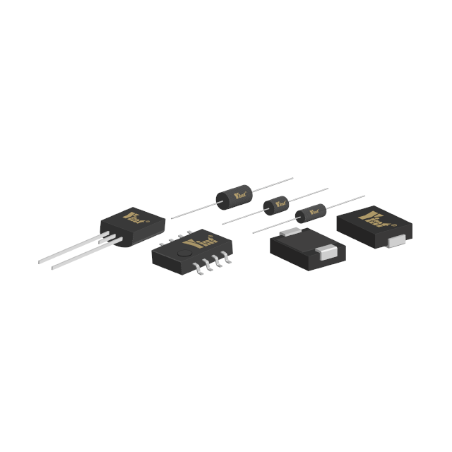
With the increasing popularity and widespread application of compound semiconductor devices, new requirements have been put forward for the packaging of compound semiconductor devices and modules due to application needs, such as low loss, low inductance, high power density, high heat dissipation performance, high integration, and multi-functions, which are giving rise to development routes different from silicon device packaging technology and product forms, with the aim of using advanced packaging technology to meet the above requirements while improving product reliability.