MOSFET gate source protection
The power MOS tube itself has many advantages, but the MOS tube has a relatively fragile ability to withstand short-term overload, especially in high-frequency applications. Therefore, when applying power MOS tubes, a reasonable protection circuit must be designed for it to improve the reliability of the device.
The power MOS tube protection circuit mainly includes the following aspects:
1) Prevent gate di/dt from being too high
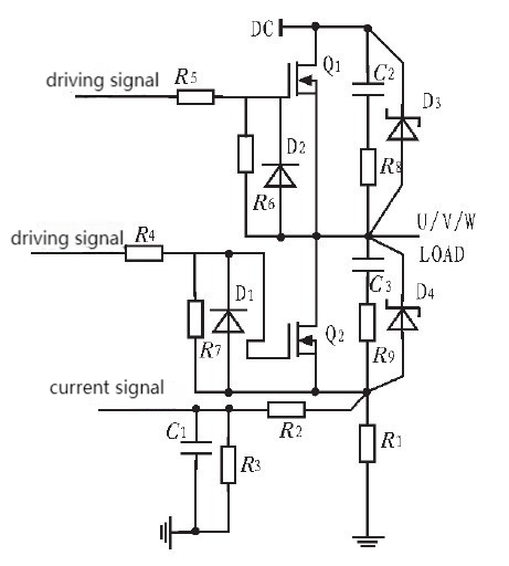
Since the driver chip is used, its output impedance is low. Directly driving the power tube will cause the driven power tube to turn on and off quickly, which may cause voltage oscillation between the drain and source of the power tube, or may cause the power tube to suffer excessive voltage. di/dt and cause misleading communication. In order to avoid the above phenomenon, a resistor is usually connected in series between the output of the MOS driver and the gate of the MOS tube. The size of the resistor is generally selected to be tens of ohms.
2) Prevent overvoltage between gate and source
Since the impedance of the gate and source is very high, a sudden change in the voltage between the drain and the source will be coupled to the gate through the interelectrode capacitance, resulting in a very high gate-source spike voltage. This voltage will cause the thin gate-source oxide layer to At the same time, it is easy for the gate to accumulate charge and cause the gate-source oxide layer to break down. Therefore, a voltage regulator tube should be connected in parallel to the gate of the MOS tube to limit the gate voltage below the voltage regulator value of the voltage regulator tube and protect the MOS tube from being Breakdown, the MOS tube gate parallel resistor is to release the gate charge and prevent charge accumulation.
3) Protect against overvoltage between drain and source
Although the drain-source breakdown voltage VDS is generally very large, if the drain-source is not protected by a protection circuit, it is also possible that a sudden change in the instantaneous current of the device switching will produce a drain spike voltage, thereby damaging the MOS tube. The faster the power tube switches, the faster the power tube switches. , the higher the overvoltage generated will be. In order to prevent device damage, protection measures such as Zener diode clamps and RC snubber circuits are usually used.
When the current is too large or a short circuit occurs, the current between the drain and source of the power MOS tube will increase rapidly and exceed the rated value. The power MOS tube must be turned off within the time specified by the overcurrent limit, otherwise the device will be Burn out, so a current sampling protection circuit is added to the main circuit. When the current reaches a certain value, the drive circuit is turned off through the protection circuit to protect the MOS tube.
The picture below shows the protection circuit of a MOS tube, from which we can clearly see the function of the protection circuit.
