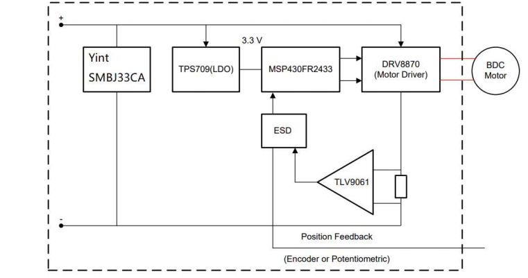
The TIDA-01588 Series is widely used in laser printers to drive and control the position of brushed DC (BDC) motors running on 3 to 6-cell Li-ion batteries, where the power supply and encoder signal lines are found to be susceptible.
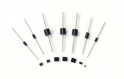
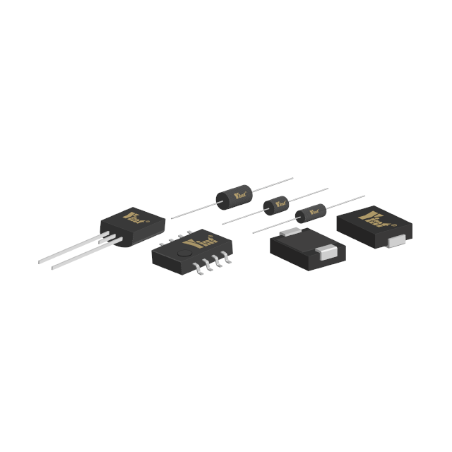
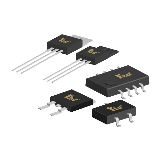
Its power port circuit protection device uses SMBJ33CA, which can well protect the power chip, and the surge at the input end has a good clamping effect, with picosecond-level response speed.

SMBJ33CA important parameters:
1、PW:600W V@11.3A clamping voltage 53.3V
2、SMD package, DO-214AA/SMB
3、Ultra-low leakage current, picosecond response
4、JESD210A International Standard
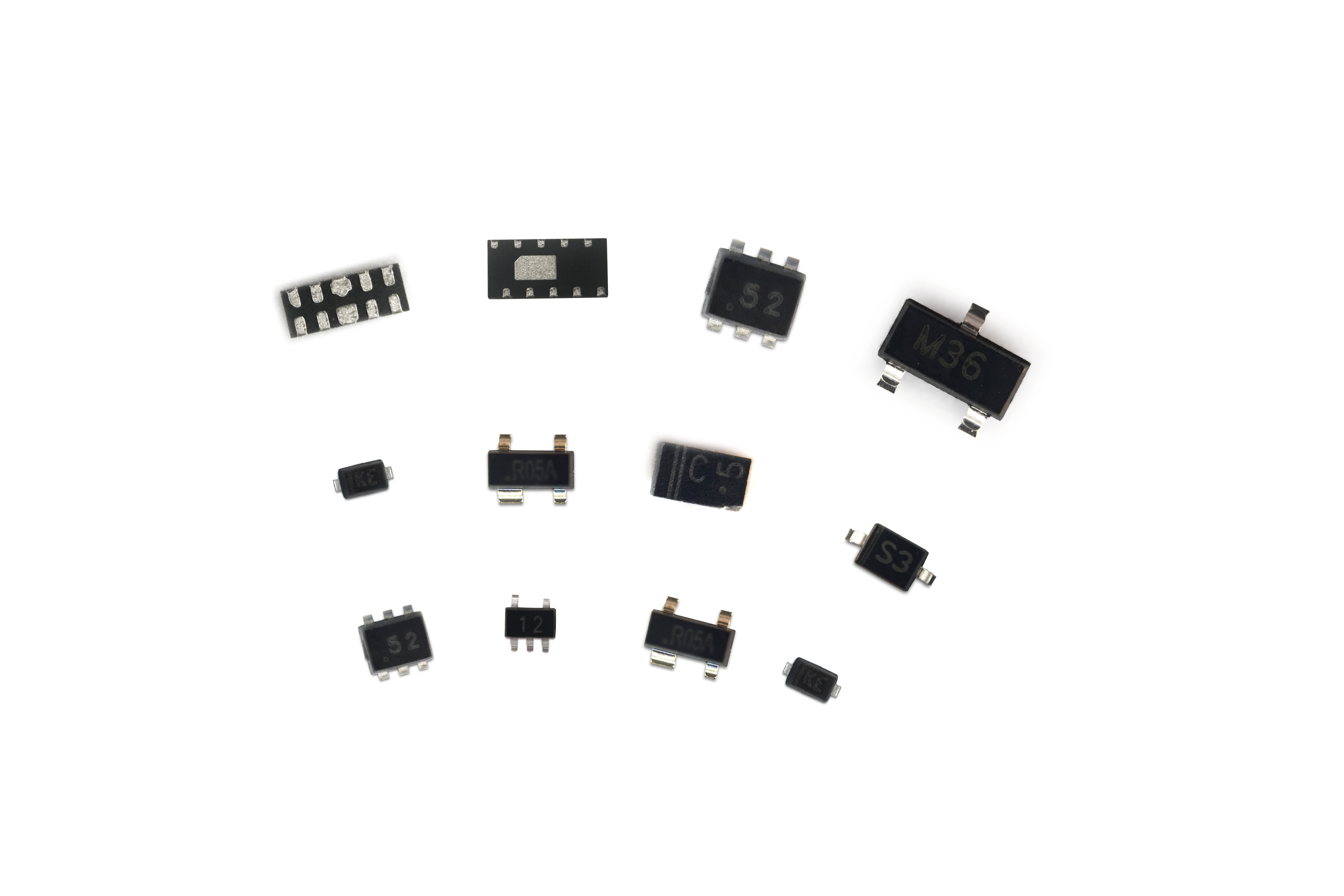
Electrostatic Protection for MSP430FR2433 Encoder A and Encoder B
Important parameters of ESDLC5V0D3B:
Vrm: 5V VC@1A 9.8V ultra-fast response nS level
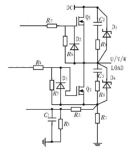
The power MOS tube itself has many advantages, but the MOS tube has a relatively fragile ability to withstand short-term overload, especially in high-frequency applications,so in the application of power MOS tubes, a reasonable protection circuit must be designed for it to improve the reliability of the device.
The power MOS tube protection circuit mainly has the following aspects:
1、Prevent gate di/dt from being too high
Due to the use of the driver chip, its output impedance is low, directly driving the power tube will cause the driven power tube to be turned on and off quickly, which may cause voltage oscillation between the drain and source of the power tube,or it may cause the power tube to suffer from excessive di/dt and cause false conduction.In order to avoid the occurrence of the above phenomenon, a resistor is usually connected in series between the output of the MOS driver and the gate of the MOS transistor, and the size of the resistor is generally selected as tens of ohms.
2、Prevent overvoltage between gate and source
Due to the high impedance between the gate and the source, a sudden change in the voltage between the drain and the source will be coupled to the gate through the inter-electrode capacitance to generate a relatively high gate-source spike voltage, which will make the very thin gate-source oxide layer breakdown.
At the same time, it is easy to accumulate charges on the gate and cause the breakdown of the gate-source oxide layer. Therefore, a Zener tube should be connected in parallel to the gate of the MOS tube to limit the gate voltage below the regulator value of the voltage tube to protect the MOS tube from being broken down. The parallel resistor on the gate of the MOS transistor is to release the gate charge and prevent the charge from accumulating.

3、Protection against overvoltage between drain and source
Although the drain-source breakdown voltage VDS is generally very large, if there is no protection circuit for the drain-source, it is also possible that the drain peak voltage will be generated due to the sudden change of the device switching current, which will damage the MOS tube, and the faster the switching speed of the power tube , the higher the overvoltage will be. To prevent device damage, protective measures such as Zener diode clamps and RC snubber circuits are usually used.When the current is too large or a short circuit occurs, the current between the drain and source of the power MOS tube will increase rapidly and exceed the rated value, and the power MOS tube must be turned off within the time specified by the overcurrent limit value, otherwise the device will be damaged. Burn out, so add a current sampling protection circuit in the main circuit, when the current reaches a certain value, turn off the drive circuit through the protection circuit to protect the MOS tube.
The figure below is the protection circuit of the MOS tube
