
 Global


1. Thoughts and Solutions to Gate Issues of SIC MOSFETs
As a new type of power semiconductor device, the SIC MOSFET has been widely applied in new energy vehicles, photovoltaics, smart grids, and other fields in recent years, driven by the maturity of its technology. With its notable advantages such as fast switching speed, low on-resistance, and high temperature resistance, it has gradually become a powerful alternative to traditional silicon-based devices
Taking new energy vehicles as an example, the application of SIC MOSFETs in on-board inverters can improve the efficiency of electric energy conversion, reduce energy loss, and thereby increase the vehicle's cruising range. In the photovoltaic field, photovoltaic inverters using SIC MOSFETs can achieve higher power density and conversion efficiency, reducing system costs
2. The importance of studying gate issues
The gate, as a crucial control terminal of the SIC MOSFET, directly affects the operational stability and lifespan of the entire device through its performance and reliability. Once the gate is damaged, the SIC MOSFET will fail to operate normally, leading to malfunctions in the entire circuit system. As a novel power semiconductor device, the SIC MOSFET has been widely applied in various fields such as new energy vehicles, photovoltaics, and smart grids in recent years due to the maturity of its technology. With its notable advantages such as fast switching speed, low on-resistance, and high temperature resistance, it has gradually become a powerful alternative to traditional silicon-based devices
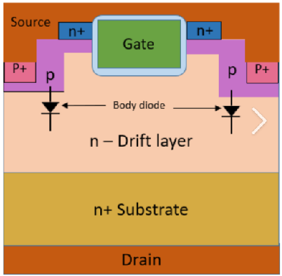
3. Overview of chip process structure
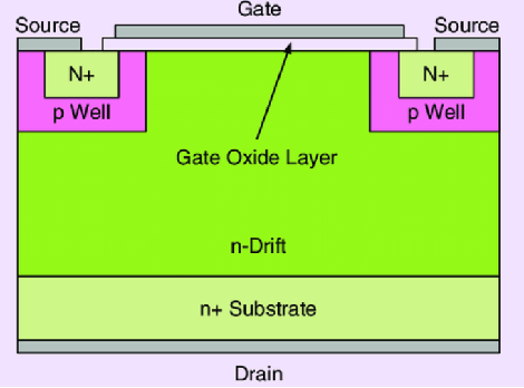
The chip process structure of SIC MOSFETs primarily comprises a substrate, epitaxial layer, source, drain, gate, and insulating layer. The substrate typically employs silicon carbide material, characterized by high thermal conductivity and high breakdown electric field strength, providing excellent physical support and electrical foundation for the device. The epitaxial layer grows atop the substrate, facilitating precise control over the electrical parameters of the device
The source and drain are located on both sides of the chip, serving as the input and output terminals for current. The gate is separated from the channel by an insulating layer, and controls the conduction and cutoff of the channel by applying voltage, thereby regulating the current. The insulating layer is usually made of materials such as silicon dioxide, and its quality and thickness have a significant impact on the performance of the gate
4. The position and role of the gate in the chip
Position:
The gate is located between the source and the drain, closely adjacent to the channel through an insulating layer. Its main function is to control the conductivity of the channel through electric field effects, achieving precise control over the on and off states of the SIC MOSFET. When a positive voltage is applied to the gate, electrons are induced in the channel, forming a conductive path, which turns on the SIC MOSFET; when the gate voltage is zero, the electrons in the channel disappear, the conductive path closes, and the SIC MOSFET is turned off
Function: The control function of the gate is akin to the on-off switch of a faucet, capable of precisely regulating the magnitude and flow (current) of water, ensuring the stable and reliable operation of SIC MOSFETs in various circuit applications
5. Analysis of the reasons for the susceptibility of the gate to damage
The mechanism of action of Miller capacitance
Due to factors such as polysilicon width, channel and trench width, G-gate oxide thickness, and PN junction doping profile, SIC MOSFETs generate parasitic capacitance, with the key Miller capacitance Cgd playing a significant role. Cgd is not constant and changes rapidly with the variation of voltage between the gate and drain
When the high-side MOSFET suddenly turns on, the drain voltage of the low-side MOSFET will momentarily increase. At this time, a current equal to the product of the Miller capacitance and the voltage change rate will flow through the Miller capacitance of the low-side MOSFET. If the gate is open-circuited, this current can only charge the underlying Cgs capacitance, which in turn leads to a sudden increase in gate voltage. When the gate voltage exceeds the threshold voltage VTH of the MOSFET, the MOSFET is prone to false turn-on. Prolonged false turn-on can damage the gate
Example of issues caused by parasitic capacitance
In a half-bridge circuit, when one MOSFET is turned on, the presence of Miller capacitance can affect the gate of the other MOSFET. For instance, in a certain switching power supply application, due to the effect of Miller capacitance, the gate voltage rises abnormally, exceeding the gate's voltage tolerance range, ultimately leading to gate breakdown and damage, rendering the entire switching power supply inoperable
6. Sources of overvoltage in external circuits
6.1 Overvoltages in external circuits can arise from various causes, such as lightning strikes, grid fluctuations, and switching operations of inductive loads. Lightning strikes can generate instantaneous high voltage pulses, which may be conducted to SIC MOSFETs through power or signal lines
6.2 During grid fluctuations, sudden voltage spikes can also pose a threat to SIC MOSFETs
6.3 When inductive loads (such as motors, transformers, etc.) are suddenly disconnected, a back electromotive force is generated, resulting in high voltage spikes. These overvoltages may be conducted through the circuit to the gate of the SIC MOSFET, causing damage to it
7. Principle of damage to gate caused by overvoltage
7.1 When the voltage applied to the gate exceeds its rated withstand voltage, the gate oxide will break down, leading to a decrease in the insulation performance between the gate and the channel, and even short-circuiting. This will cause the gate to lose its control over the channel, rendering the SIC MOSFET unable to operate normally. In severe cases, it may result in permanent damage to the device
7.2 Overvoltage may also induce thermal effects within the gate, causing a sharp increase in the temperature of the gate material, leading to performance degradation of the material and further exacerbating the damage to the gate
Operating temperature characteristics of SIC MOSFETs
Although SIC MOSFETs exhibit good high-temperature performance, their performance parameters still undergo changes in high-temperature environments. As the temperature rises, the on-resistance of SIC MOSFETs increases, the switching speed decreases, and the leakage current also increases. These parameter variations lead to increased power consumption of the device, generating more heat, which further exacerbates the temperature rise.
When the temperature exceeds a certain threshold, it will affect the material and structure of the gate, reducing the reliability of the gate
The impact of high temperature on gate materials and structures
High temperatures can degrade the performance of the insulating material of the gate, leading to a decrease in the insulation resistance between the gate and the channel, thereby increasing the risk of leakage. Additionally, high temperatures may cause thermal expansion of the gate's metallic material, potentially leading to loosening or fracture of the connections between the gate and other components, thus affecting the normal operation of the gate.
In some high-temperature application scenarios, such as electronic devices inside the engine compartment of automobiles, the SIC MOSFETs are exposed to high temperatures for extended periods, significantly increasing the probability of gate damage
8. Manufacturing process defects
Common manufacturing process issues
During the manufacturing process of SIC MOSFETs, some process defects may occur, such as pinholes in the gate oxide layer, impurity contamination, and lithography deviations. These defects can lead to uneven thickness of the gate oxide layer and locally high electric field strength, thereby reducing the voltage withstand capability of the gate.
Impurity contamination may alter the electrical properties of gate materials, affecting the normal operation of the gate. Photolithography deviations may lead to insufficient dimensional accuracy of the gate, affecting the performance consistency of the device
How do process defects lead to gate damage
Pinholes in the gate oxide layer can become leakage paths for current. When current passes through the pinholes, it can generate localized heating, leading to further damage to the oxide layer.
Impurity contamination can cause changes in the resistivity of gate materials, affecting the electric field distribution of the gate and increasing the risk of gate breakdown
Inconsistencies in gate dimensions caused by lithography deviations can lead to differences in gate performance across different devices. In practical applications, gates with poorer performance are more susceptible to damage
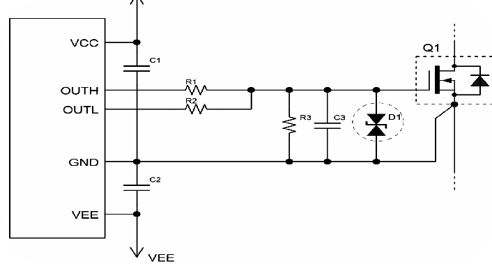
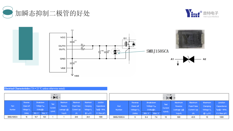
Introduction to basic working principles
SMBJ1505CA is an efficient circuit protection device, whose working principle is based on the avalanche breakdown effect of the PN junction. When the voltage across the TVS exceeds its breakdown voltage, the TVS will quickly turn on, clamping the overvoltage to a lower level, thereby protecting the protected device from the impact of excessively high voltage. In the circuit, the TVS is usually connected in parallel with the gate of the protected SIC MOSFET. When a transient overvoltage occurs, the TVS responds in an extremely short time (usually in nanoseconds), bypassing the overvoltage to ground, keeping the gate voltage within a safe range
The SMBJ1505CA transient suppression diode is specifically designed for gate protection of SIC MOSFETs. Its forward breakdown voltage is typically set at around 15V, while the reverse breakdown voltage is set at around -5V. This voltage setting matches the gate operating voltage range of SIC MOSFETs, effectively protecting the gate from damage caused by forward and reverse overvoltages. This diode features fast response time, low dynamic resistance, and high pulse power withstanding capability. The fast response time ensures timely action at the moment of overvoltage occurrence, the low dynamic resistance allows the clamping voltage to be as close to the breakdown voltage as possible, and the high pulse power withstanding capability ensures that the diode will not be damaged when subjected to high-current pulses
9. Reasons for using SMBJ1505CA
9.1 Preventing gate voltage fluctuations caused by crosstalk
In applications such as half-bridge circuits, the switching action of a SIC MOSFET module can cause fluctuations in the gate-source voltage of another module's switch, leading to crosstalk issues. Positive crosstalk may result in a positive increase in gate voltage, which, if exceeding the threshold, can lead to false turn-on; negative crosstalk may cause a negative increase in gate voltage, exceeding the negative voltage tolerance limit and leading to gate breakdown. The SMBJ1505CA transient suppression diode can effectively suppress the gate voltage fluctuations caused by crosstalk. When the gate voltage experiences abnormal increases or decreases, the TVS will quickly turn on, clamping the voltage within a safe range to prevent false turn-on and gate breakdown
9.2 Addressing the threat of transient overvoltages
As mentioned earlier, external circuits are threatened by various transient overvoltages, such as those generated by lightning strikes, grid fluctuations, and inductive load switching. These overvoltages may momentarily exceed the voltage rating of the SIC MOSFET gate, causing irreversible damage to the gate.
The transient suppression diode can respond quickly to the occurrence of overvoltage, limiting it to a safe range, providing reliable protection for the SIC MOSFET gate, and ensuring the device operates normally in harsh electrical environments
The benefits of adding a transient voltage suppressor diode
By suppressing overvoltage and crosstalk, transient suppression diodes can effectively reduce the electrical stress on the gate, lower the risk of gate damage, and thereby enhance the reliability and stability of the SIC MOSFET gate. This contributes to extending the service life of SIC MOSFETs, reducing the occurrence of equipment failures, and improving the reliability of the entire circuit system.
In fields such as industrial automation and power electronics, the reliability and stability of equipment are crucial. Using transient suppression diodes to protect the gate can ensure long-term stable operation of the equipment and reduce maintenance costs
 Hot News


 沪公网安备31011702889749号

