
 Global


Silicon Carbide MOSFETs (Metal-Oxide-Semiconductor Field-Effect Transistors) offer higher breakdown electric field strength and lower leakage current compared to traditional silicon MOSFETs.
This inherently provides better resistance to electrostatic discharge (ESD) issues to some extent. However, to further address ESD concerns, the following common methods can be employed:
1. Design Appropriate Protection Circuits: Implement ESD protection at the input and output terminals of the MOSFET, such as using TVS diodes or ESD discharge tubes. These protection circuits can absorb and dissipate electrostatic energy, safeguarding the MOSFET from ESD damage.
2. Avoid Environments Prone to Electrostatic Generation and Accumulation: Adopt suitable environmental control measures, such as proper grounding and anti-static equipment, to reduce the likelihood of electrostatic generation and accumulation. For example, use anti-static workstations on production lines and wear anti-static clothing.
3. Dynamic Electrical Protection: For situations where ESD may damage the MOSFET, such as when connecting or disconnecting high-voltage power sources, employ dynamic protection methods like reset circuits and sensing circuits to mitigate the impact of ESD on the MOSFET.
4. Optimize Packaging and Connection Methods: Select appropriate packaging and connection methods to minimize the conduction and accumulation of static electricity. Effective packaging and connection designs can provide better isolation and shielding, reducing the influence of ESD on the MOSFET.
5. Training and Precautions: Provide relevant training and guidelines for engineers and operators working with silicon carbide MOSFETs, educating them on proper handling and operation of the devices to minimize the risk of ESD damage.
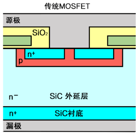
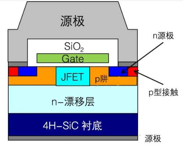
Structural Comparison: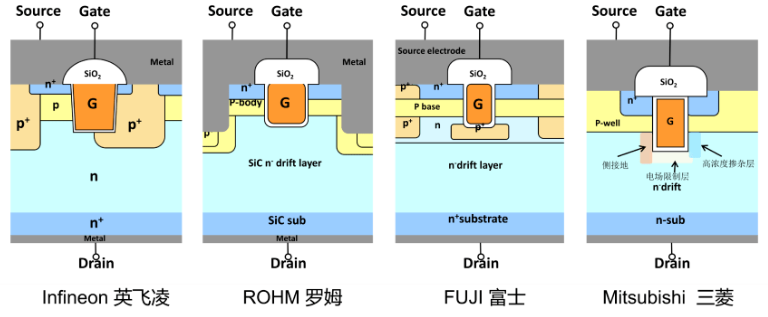
These methods can help better address ESD issues in silicon carbide MOSFETs, enhancing device reliability and stability.
 Hot News


 沪公网安备31011702889749号

