
 Global


Ion implantation in silicon carbide (SiC) is a technique used to introduce specific impurity atoms into silicon carbide material. Ion implantation typically involves injecting the desired dopants into the silicon carbide crystal using high-energy ion beams.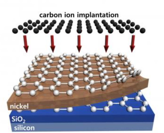
The ion implantation process includes the following steps:
1. Select the target impurity atoms to be implanted, such as boron (B), nitrogen (N), or phosphorus (P).
2. Prepare the silicon carbide substrate and thin film layers to support and protect the ion implantation process.
3. Use an ion implanter to introduce high-energy ion beams into the silicon carbide material. The ion beams penetrate the thin film layers and are implanted into the silicon carbide crystal.
4. After implantation, the material is converted into functional devices through additional process steps such as annealing, cleaning, and electrode formation.
Selective doping technology is a method to control the ion implantation process. It utilizes photolithography and thin film techniques to precisely define and control the ion implantation regions during manufacturing. By coating photoresist in specific areas and performing steps like exposure and development, a mask can be created in the target regions. This mask prevents ions from entering the protected areas of the material, enabling selective doping. Selective doping technology can be used to form specific doped regions in silicon carbide materials, thereby optimizing the material's electronic properties and device performance.
In summary, ion implantation in silicon carbide is a technique for introducing specific impurity atoms into the material, while selective doping technology is a method to control the ion implantation process, achieving doping in specific regions through masking techniques to optimize the performance of silicon carbide materials.
 Hot News


 沪公网安备31011702889749号

