1. Electrostatic Discharge Protection Requirements Analysis for Medical Monitor ECG Signal Pathways
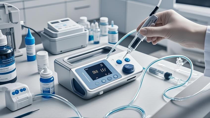
- The electrocardiogram (ECG) signal pathway of a medical monitor is responsible for acquiring, amplifying, and processing weak bioelectric signals originating from the patient's body surface.
- Typical ECG signal amplitude ranges from 0.5 mV to 5 mV, with frequency components concentrated between 0.05 Hz and 150 Hz. The front end of this pathway typically includes a high-input impedance (>100 MΩ) instrumentation amplifier, a Right Leg Drive (RLD) circuit, and multi-stage filter networks.
- Due to direct contact with the human body, ECG lead interfaces must comply with IEC 60601-1-2 (Electromagnetic Compatibility of Medical Electrical Equipment) and IEC 61000-4-2 (Electrostatic Discharge Immunity) standards. They are required to withstand transient voltage surges of contact discharge ±8 kV and air discharge ±15 kV.
- Traditional protection solutions use multilayer varistors (MLV) or transient voltage suppression diodes (TVS). However, their inherent parasitic capacitance (typically >10 pF) forms a low-pass filter with the input impedance of the front-end amplifier. This leads to the attenuation of high-frequency components of the ECG signal, affecting waveform fidelity and diagnostic accuracy.
2. NRESDTLC5V0D8B Device Electrical Characteristics
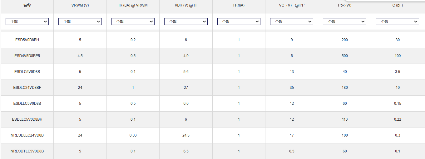
The NRESDTLC5V0D8B is an integrated bidirectional electrostatic protection diode manufactured using advanced silicon semiconductor technology.
Core electrical parameters include:
- Reverse standoff voltage (Working Voltage, VRWM) is 5.0V ±5%, compatible with the common ±2.5V to ±5V power supply range of ECG signal conditioning circuits.
- Clamping voltage (Clamping Voltage, VC) has a typical value of 9.5V under an 8A pulse current (IPP), ensuring transient energy is quickly shunted to the ground plane.
- The key parameter, parasitic capacitance (CD), is as low as 0.15 pF (test condition: 1 MHz, 0V bias). This value is 1-2 orders of magnitude lower than traditional TVS devices.
- The device uses a DFN1006 (1.0 mm × 0.6 mm) package, with a footprint of only 0.6 mm², aligning with the trend of medical device miniaturization.
- Its internal structure features a symmetric back-to-back Zener diode layout, achieving bidirectional voltage clamping without needing to consider polarity during connection, thus simplifying PCB layout and assembly processes.
3. Impact Mechanism of Low Parasitic Capacitance on ECG Signal Integrity
3.1 The input equivalent circuit of the ECG signal pathway can be modeled as a parallel network of the source impedance ZS (human body-electrode contact impedance, approximately 10 kΩ to 100 kΩ), the protective device's parasitic capacitance CD, and the amplifier's input capacitance CIN.
3.2 The transfer function of this network is H(s) = 1 / (1 + s·RS·(CD + CIN)), where s is the complex frequency variable.
3.3 When CD = 0.15 pF, CIN = 5 pF, RS = 50 kΩ, the system's -3 dB cutoff frequency fc = 1/(2π·RS·(CD+CIN)) ≈ 618 kHz, which is far higher than the maximum ECG signal frequency of 150 Hz.
3.4 Using a traditional TVS with CD = 10 pF, fc would drop to approximately 309 kHz. Although still above 150 Hz, changes in phase delay and group delay might affect the synchronization of multi-channel ECG.
3.5 A low CD can reduce the shift in the high-pass filter cutoff frequency within AC-coupled circuits, ensuring effective suppression of baseline drift below 0.05 Hz.
4. Layout and Grounding Strategies in ECG Front-End Circuits
4.1 It is recommended to place the NRESDTLC5V0D8B on the signal path after the ECG lead connector and before the instrumentation amplifier's input pins. A symmetrical layout should be used to maintain the Common Mode Rejection Ratio (CMRR).
4.2 Each differential input channel (e.g., RA, LA, LL) needs to be independently configured with a protection device. The right leg drive feedback path also requires separate protection.
4.3 PCB routing should follow these principles: the protective device's ground pin should connect to a low-impedance ground layer via the shortest path (<2 mm). This ground layer should connect to the digital ground at a single point through a ferrite bead or 0 Ω resistor to avoid contaminating the analog reference ground with transient currents.
4.4 Power rails (+5V/-5V) should be configured with decoupling capacitors (100 nF ceramic capacitor in parallel with a 10 µF tantalum capacitor) to prevent power supply disturbances caused by ESD events. The device's operating temperature range is -55°C to +125°C, meeting the reliability margin required for medical environments (typically 0°C to 40°C).
5. Extended Application: RF Antenna Port Protection for 2.4 GHz Wireless Monitoring Devices
- The NRESDTLC5V0D8B is also suitable for ESD protection at the 2.4 GHz antenna port of medical monitors integrated with wireless transmission modules (e.g., Bluetooth/BLE, Wi-Fi).
- In RF systems, the protection device is connected in parallel between the antenna feed line and ground. Its capacitance CD and the antenna impedance (typically 50 Ω) form a high-pass network.
- Insertion Loss (IL) can be estimated by the formula IL(dB) = 10·log10(1 + (ω·CD·Z0)2), where ω = 2πf, Z0 = 50 Ω.
- At f = 2.4 GHz, the theoretical insertion loss for CD = 0.15 pF is only 0.017 dB, which has a negligible impact on the antenna Voltage Standing Wave Ratio (VSWR) (typical value < 1.05:1).
- The NRESDTLC5V0D8B can withstand repeated impacts according to IEC 61000-4-2 Level 4 (contact discharge ±8 kV), ensuring the continuous stability of the wireless link in medical environments.
6. Testing Verification and Compliance Considerations
- Use an ESD simulator compliant with the IEC 61000-4-2 standard to test an ECG prototype integrated with the NRESDTLC5V0D8B.
Test Configuration:
- Contact discharge: ±2 kV, ±4 kV, ±8 kV, applied to all lead interfaces and the device casing.
- Monitoring indicators include: ECG output waveform Total Harmonic Distortion (THD < 1%), Common Mode Rejection Ratio (CMRR > 100 dB @ 50 Hz), baseline recovery time (< 200 ms post-ESD).
- Radio Frequency performance verification is required: Use a Vector Network Analyzer to measure the S11 parameter of the 2.4 GHz antenna port before and after the protection device is installed, ensuring return loss is better than -10 dB.
- The design must pass Medical Device Quality Management System (ISO 13485) certification and meet the Electromagnetic Compatibility (EMC) requirements for FDA 510(k) or CE Mark.
Conclusion: The NRESDTLC5V0D8B, with its 0.15 pF ultra-low parasitic capacitance, 5V working voltage, and DFN1006 miniature package, provides a high-fidelity, highly reliable electrostatic protection solution for the ECG signal pathways of medical monitors.

 Global


 Hot News


 沪公网安备31011702889749号

