
 Global


《Yinte Electronics "pushes for you》
According to reports, German silicon-based gallium nitride expert ALLOSSemiconductors announced a collaboration with a research team from King Abdullah University of Science and Technology (KAUST) in Saudi Arabia to jointly develop efficient silicon-based InGaN red MicroLEDs. It is understood that issues such as lattice mismatch and quantum confined Stark effect (QCSE) limit the practical use of red nitrogen based LEDs in industrial applications, and this collaboration between ALLOS and KAUST will aim to address these fundamental problems.
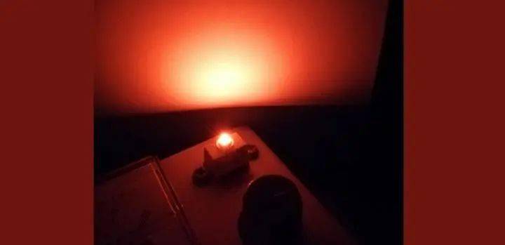
Image source: KAUST
It is worth noting that in the field of MicroLED displays, in addition to blue and green LEDs, MicroLED displays also have a strong demand for growing red LEDs on large-sized wafers, with the aim of reducing manufacturing complexity and costs.
It is reported that the KAUST team has made some breakthroughs in developing efficient InGaN based red MicroLEDs with forward voltage below 2.5V by adopting Local Strain Compensation and improved MOCVD reactor design. They have grown red LEDs on sapphire substrates and Ga2O3 (gallium oxide) substrates.
In order to develop potential high-performance red LEDs using wafer level (especially large-sized wafers) engineering strain technology, the KAUST team and ALLOS have jointly extended their research work to silicon substrates. With the ability to expand wafers to 300mm and process them on silicon substrate production lines, the cooperation between the two parties will accelerate the mass production process. For MicroLED displays, especially for single-chip integrated MicroLED displays used in AR devices, this will be another important assist.
The KAUST team and ALLOS will fully utilize their respective expertise to address strain issues, optimize the crystal growth conditions of silicon-based gallium nitride and red LEDs, and ultimately achieve the growth of red LED stacks on silicon-based gallium nitride buffer layers.
 Hot News


 沪公网安备31011702889749号

