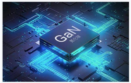


GaN Protect Gallium Nitride
Integrating multiple power electronic devices onto a gallium nitride chip can effectively improve product charging speed, efficiency, reliability, and cost-effectiveness.
GaN gallium nitride is the key to improving the overall system performance, creating circuit components that approach the "ideal switch" - a circuit component that can convert the minimum energy digital signal into lossless power transmission.
Both "full bridge" and "half bridge" circuit designs can be supported by gallium nitride power chips.
Gallium nitride power chips have a highly applicable power range and functionality, covering mobile fast chargers, data centers, consumer markets, renewable energy, and electric vehicles/electric vehicles. Their advantages can be highlighted in various applications ranging from tens of watts to over kilowatts!
The GaN Protect team is developing a new generation of power protection devices, embedded modules, and standalone applications!
Theoretical advantages of GaN Protect:
Smaller size: GaN Protect devices can achieve charging speeds 2.7 to 3 times faster than traditional silicon chips, with only half the size and weight of the former. In terms of energy savings, it can save up to 40% of energy.
Faster speed: The integrated design of gallium nitride power IC makes it very easy to use. The layout and control are very simple through simple "digital input, power output" operations.
More environmentally friendly: Due to the small die size, fewer manufacturing process steps, and functional integration, the carbon dioxide emissions during the manufacturing of gallium nitride power chips are 10 times lower than those of charging solutions for silicon devices.
Reliability: GaN Protect devices comply with the dual carbon policy, have lower internal resistance, and will generate less heat, resulting in lower risk
What is GaN Protect? It is a trademark registered by the R&D team of Yin Te, which uses GaN material to protect devices!

 Hot News