
 Global


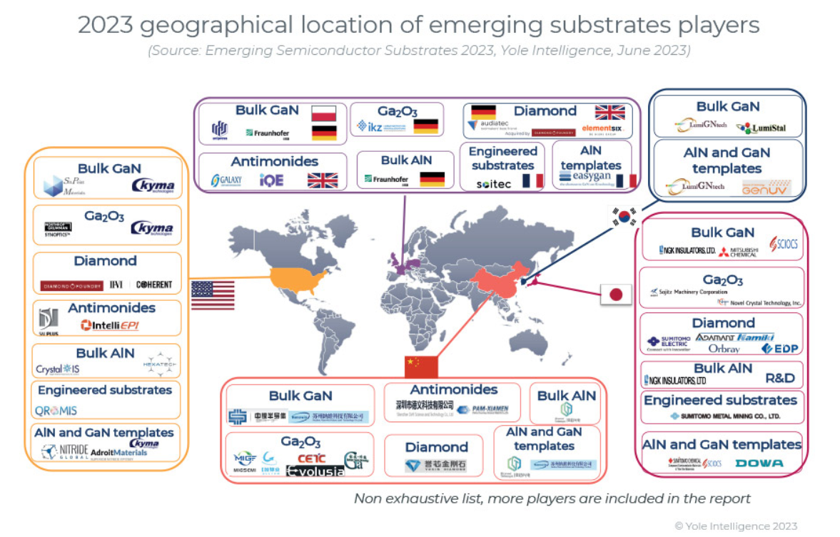
Due to the need to improve performance and cost constraints, new materials, platforms, and designs are constantly being researched in the semiconductor industry. In the past decade, some compound semiconductors, such as gallium arsenide (GaAs) for radio frequency (RF) and silicon carbide (SiC) for power electronics, have successfully competed with silicon and entered the mass market. So, which emerging semiconductor substrate will be the next game changer? In its latest report "Emerging Semiconductor Substrates 2023", Yole Intelligence (part of Yole Group) investigates the technological status of emerging semiconductor substrates, including gallium antimonide (GaSb), indium antimonide (InSb), bulk gallium nitride (GaN), gallium oxide (Ga2O3), bulk aluminum nitride (AlN), and diamond, as well as engineered substrates and templates. In addition, market research and strategic consulting firms have also studied various potential applications such as power electronics, radio frequency, and photonics, including laser diodes, light emitting diodes (LEDs), sensors, and detectors. Including GaSb, InSb, bulk GaN, Ga2O3, bulk AlN, and diamonds, as well as engineering substrates and templates, the value of the emerging substrate market is estimated to be $63.6 million in 2022, and is projected to grow at a compound annual growth rate of 27% to over $264.5 million by 2028.
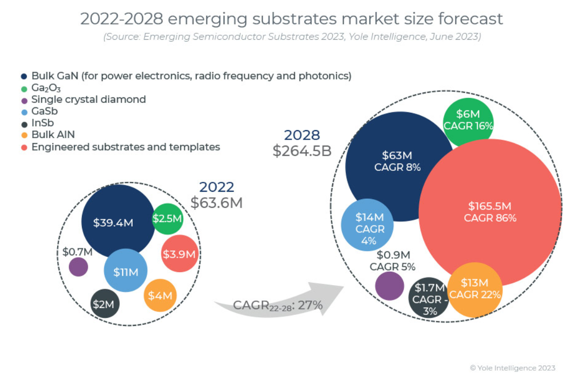
Dr. Taha Ayari, compound semiconductor and emerging substrate technology and market analyst at Yole Intelligence, pointed out that the power electronics market is still dominated by silicon-based technology, driven by various applications such as EV/HEV (electric and hybrid vehicles), renewable energy, and power sources. Nevertheless, wide bandgap materials SiC and GaN (transverse GaN HEMTs on silicon or sapphire) have penetrated the power electronics market through a long development process and are expected to account for over 25% of the power electronics market by 2028, "he added. Thanks to this momentum, Yole Intelligence expects bulk GaN for vertical GaN devices and engineering substrates (SmartSiC from Soitec, SiCkrest from SICOXS, and QST from Qromis) to grow over the next five years
On the other hand, driven by high-end and niche military applications, the optoelectronics market is steadily growing with gasb based devices such as infrared (IR) lasers and imagers. The report also reviewed the market situation of InSb. The market for bulk GaN substrates in consumer, industrial, and automotive applications is considered stable, and industrial applications will receive greater impetus. During the pandemic, UVC disinfection/purification systems began using bulk AlN substrates. This will drive the compound annual growth rate (CAGR) of the AlN substrate market to 22% between 2022 and 2028, the highest among all emerging photonic substrates. Dr. Ali Jaffal, a compound semiconductor and emerging substrate technology and market analyst at Yole Intelligence, pointed out that "emerging substrate activities mainly focus on technology development to achieve better material quality, higher output, and lower production costs." "Of course, this push needs to be supported by market demand and batch applications, which define the correct specifications for different substrates. Combined with increasing substrate diameters, this will drive the emerging substrate industry towards large-scale production
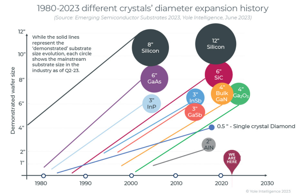
For the power electronics industry, mature foundries require a minimum wafer size of 6 inches to produce in large quantities. This prompts substrate manufacturers to optimize manufacturing technology and increase wafer size. For diamonds, methods have been developed to obtain inlaid diamonds up to 28mm x 28mm from etched spacing density (EDP), as well as heterogeneous diamonds grown to a diameter of approximately 6 inches on Orbray or Audiatec silicon or sapphire substrates. In addition, the use of hydride vapor phase epitaxy (HVPE) and other techniques has demonstrated 6-inch bulk GaN substrates, although more work is still needed to improve material quality and meet application requirements. Similarly, for Ga2O3, different melt growth techniques are being used, with EFG (Edge Defined Film Growth) being the most promising for obtaining 6-inch wafers with acceptable material quality in mass production. For engineering substrates, advanced splitting and bonding techniques are used to overcome the challenges of larger single crystal substrates and better material quality. Tags: Substrates Visit: www.yolegroup.com
 Hot News


 沪公网安备31011702889749号

