


 Global









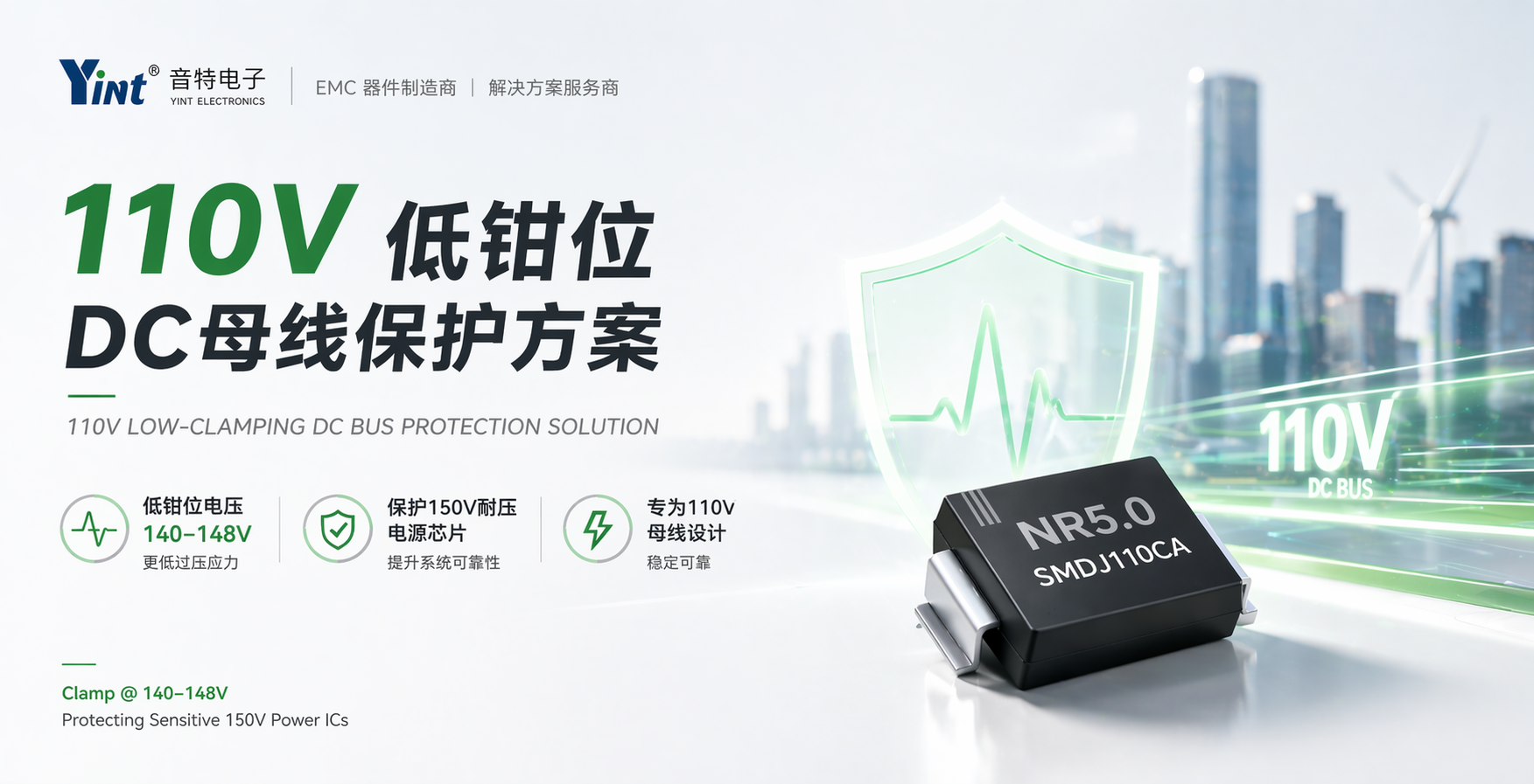
In 110V-class bus systems, the absolute maximum voltage tolerance of a large number of DC-DC/power management chips on the market is concentrated at the 150V level. This means that input protection must strictly limit the chip pin voltage to a safe window close to but not exceeding 150V when surges, hot-plugging, or harness-induced spikes occur. Traditional TVS devices often have a high clamping voltage under large currents, causing the chip-side voltage to still potentially exceed the window, leading to latent damage or direct failure.
As power chip processes evolve toward smaller line widths and higher integration, the margins of gate oxide, drift regions, and protection structures within the device are further compressed. At the same time, chips often integrate more high-voltage switching devices and control circuits. Any abnormal input spike may trigger: gate oxide stress accumulation, ESD/surge protection structure breakdown or leakage increase; internal parasitic structure conduction caused by overvoltage triggering, leading to localized overheating; parameter drift induced by repeated transients, resulting in latent failures that are "functional but unreliable."
The 110V bus often involves long wire harnesses, large loop inductance, and high di/dt from fast-switching power stages. During hot-plugging, load transients, relay switching, or external surge coupling, spike energy is released concentratedly at the input; if the clamping voltage of the protection device is not low enough or the response path is not short enough, the spike will be directly applied to the chip pins.
The design goal of the NR5.0SMDJ110CA is not to "absorb all surge energy," but rather to clamp the voltage as low and as stable as possible within the system's acceptable energy range, thereby providing a larger safety margin for DC-DC/power chips with a 150V withstand voltage.
 |
 |
 |
 |
||||
|---|---|---|---|---|---|---|---|
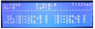
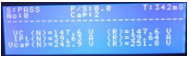
| VC1 | VC2 | VC1 | VC2 | VC1 | VC2 | VC1 | VC2 |
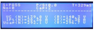
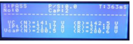
| 139.8V | 140.3V | 141.7V | 142.5V | 144.0V | 144.6V | 146.0V | 146.6V |
| IPP1 | IPP2 | IPP1 | IPP2 | IPP1 | IPP2 | IPP1 | IPP2 |
| 28.36A | 28.38A | 31.17A | 31.18A | 33.97A | 33.98A | 36.75A | 36.76A |
 |
 |
||||||
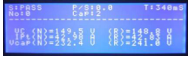
| VC1 | VC2 | VC1 | VC2 | ||||
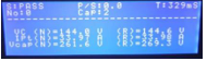
| 147.6V | 147.6V | 149.5V | 148.8V | ||||
| IPP1 | IPP2 | IPP1 | IPP2 | ||||
| 39.63A | 39.64A | 42.98A | 42.83A | ||||
 |
 |
 |
|||
|---|---|---|---|---|---|
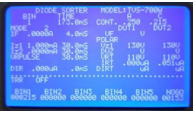
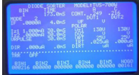
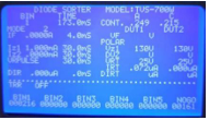
| VBR1 | VBR2 | VBR1 | VBR2 | VBR1 | VBR2 |
| 130V | 130V | 130V | 130V | 130V | 130V |
| IR1 | IR2 | IR1 | IR2 | IR1 | IR2 |
| 0.000uA | 0.051uA | 0.025uA | 0.000uA | 0.072uA | 0.000uA |
| Surge Voltage | |
|
|
|||
|---|---|---|---|---|---|---|
| Vc@Ippmax V | Ippmax A | Vc@Ippmax V | Ippmax A | Vc@Ippmax V | Ippmax A | |
| 0.8KV | 140V | 288A | 142V | 296A | 144V | 296A |
| 0.9KV | 142V | 226A | 142V | 344A | 146V | 336A |
| 1.0KV | 144V | 392A | 144V | 384A | 146V | 384A |
| 1.1KV | 146V | 432A | 146V | 432A | 146V | 432A |
| 1.2KV | 148V | 472A | 146V | 480A | 146V | 462A |
Under 1.2/50μs & 8/20μs surge conditions, test capture shows that the device's Vc@Ippmax falls approximately in the 140–148V range under 0.8–1.2kV stress (samples 2/3/4). In routine electrical testing, VBR is approximately 130V class, and the device capacitance test sample is about 876.671pF.
TVS should be placed as close as possible to the input pin of the protected chip and the return ground, with short traces and a small loop.
2. A small resistor / ferrite bead / fuse can be placed between the TVS and the bus to achieve energy limiting and graded protection (selected based on system loss tolerance).
3. For long harness applications, it is recommended to add a primary "coarse protection" at the interface side, and use this device for "fine clamping" near the chip on the board.
This low-clamping TVS device is designed for 110V DC bus systems and is suitable for DC-DC input protection scenarios that require high power supply reliability.
In the power architecture, it can be used for the input protection of DC-DC power supplies with a chip withstand voltage rating of 150V, reducing the direct impact of surges and transient spikes on the power chip. In industrial power supplies and two-wheeled or three-wheeled electric vehicle systems, it can be applied to the front-end protection between the high-voltage battery pack and the DC-DC module. In control systems such as motor drives, fans, pumps, and compressors, it is suitable for surge suppression and stability improvement at the auxiliary power input.
Additionally, in energy storage and photovoltaic systems, this solution is well-suited for bus input protection scenarios with voltage levels ranging from 100V to 120V. However, system evaluation and device selection should be performed based on the actual surge level.
In traditional designs, TVS devices typically aim to absorb surge energy as the primary objective, but in practical applications, the more critical aspect is the precise protection of the voltage withstand window of the power supply chip. The low clamping voltage design approach has a clear advantage in this regard.
| Comparison Dimension | Traditional TVS (Common Solution) | Low-Clamping TVS (NR5.0SMDJ110CA) |
|---|---|---|
| Design Objective | Primarily withstand surge energy | Core focus on controlling clamping voltage to match chip withstand voltage window |
| Clamping Performance | Higher clamping voltage under high current, risk of exceeding chip withstand voltage | Test captures Vc@Ippmax approximately 140–148V (0.8–1.2kV surge) |
| System Reliability | May cause "withstands surge but damages chip" hidden failure | More conducive to reducing overvoltage stress and long-term drift risk (needs to match system surge level) |
During the system selection process, it is recommended to prioritize application in power architectures with a "bus nominal voltage of 110V and chip withstand voltage of 150V" to achieve proper matching between the clamping voltage and the device withstand voltage window.
For application environments with higher-level surges or repeated impacts, board-level testing should be used to verify device capability and evaluate design margins to ensure long-term system reliability.
In terms of PCB layout, priority should be given to ensuring that the TVS device's return path is short, low-impedance, and direct, avoiding long common-ground paths with high-current switching loops to reduce the impact of parasitic parameters on protection effectiveness. Additionally, for systems with long wire harnesses or high-inductance loops, a graded protection strategy at both the interface side and the chip side is recommended to further enhance overall surge immunity.
Summary
The NR5.0SMDJ110CA is designed for 110V bus power systems, focusing on "protecting power chips with a 150V withstand voltage window." By employing a lower clamping strategy, it reduces the clamping voltage to approximately 140–148V (as captured in testing) under typical surge conditions, helping customers reduce input overvoltage stress and minimize the risk of latent failures. It is recommended to optimize protection based on system surge levels and layout return paths to achieve "verifiable and reproducible" protection performance.
 Hot News


 沪公网安备31011702889749号