


 Global









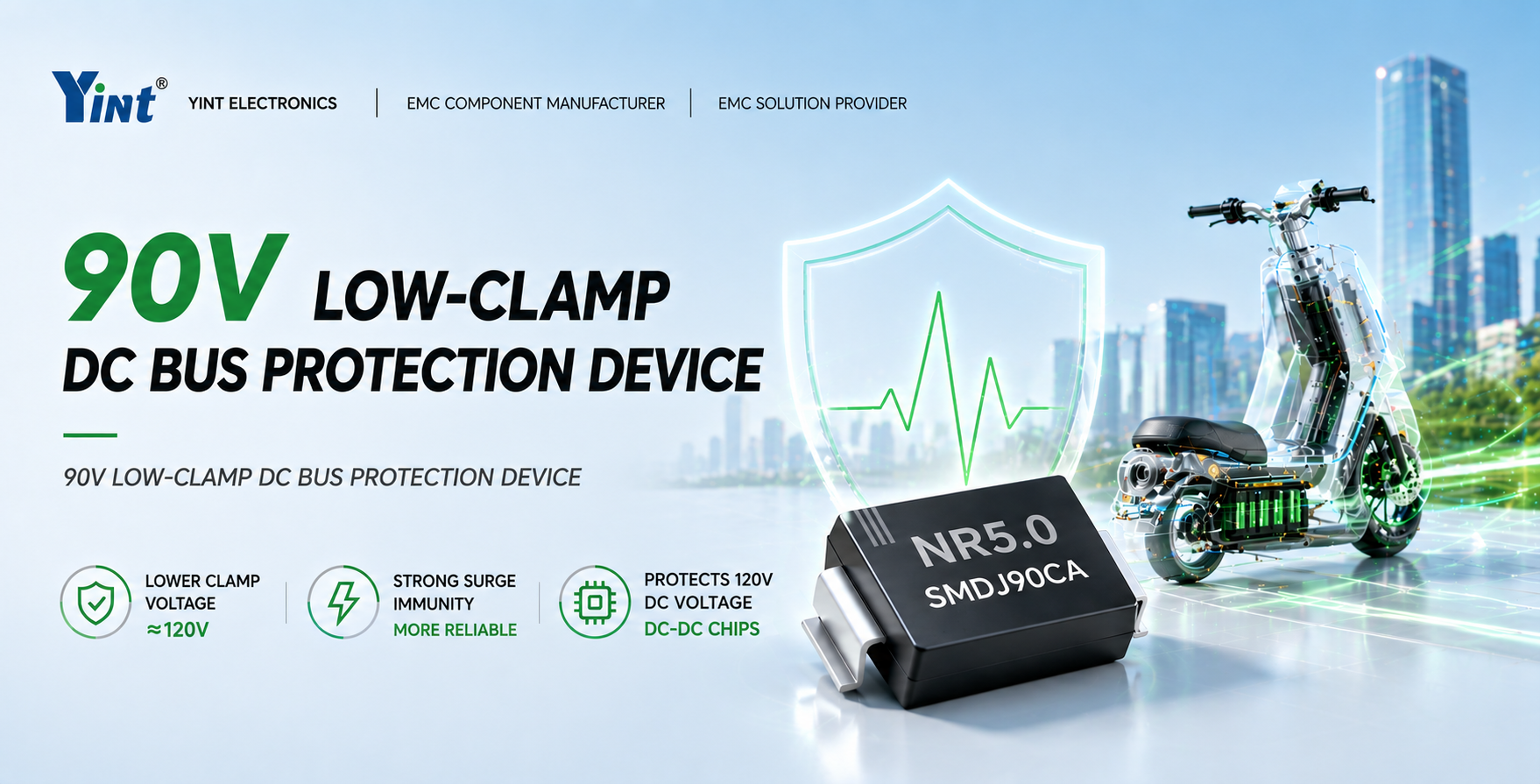
NR5.0SMDJ90CA is a "low clamping" surge/transient protection device developed for 90V bus systems. Its design goal is not simply to pursue higher peak power, but to clamp the bus voltage near the safe window of 120V withstand voltage DC-DC power chips under critical surge current conditions, thereby significantly reducing the risks of chip breakdown, gate oxide stress, avalanche degradation, and latent failure.
In actual system operation, conditions such as motor feedback, contactor and relay switching, wiring harness parasitic inductance, and load transients continuously introduce transient shocks on the bus side. These processes are typically accompanied by high di/dt and dv/dt characteristics.
It should be noted that transient risks are not entirely determined by the peak amplitude itself. Compared to traditional high-amplitude shocks, the more destructive transients currently are often those with faster rising edges and more concentrated energy. Such fast spikes are more likely to act on localized weak areas inside the power supply chip, thereby increasing the risk of device damage.
In 90V DC bus applications, power systems typically select DC-DC chips with a voltage rating of 120V, or adopt solutions with integrated high-voltage MOSFETs and rectifier structures. This voltage rating provides a certain design margin under steady-state conditions, but under surge conditions, its safety window is relatively limited.
When the bus voltage is raised close to or exceeds the chip's voltage rating during transient processes, the device enters an avalanche or overvoltage operating region. Although this process may not immediately cause functional failure, it leads to continuous thermal stress accumulation and has a long-term impact on device lifetime, thereby reducing overall system reliability.
With the continuous advancement of semiconductor processes toward smaller line widths, thinner gate oxide layers, and higher integration, the electric field distribution characteristics of devices under transient surge conditions have undergone significant changes. The effect of localized electric field concentration has become more pronounced, making devices more sensitive to ESD and surge events.
Against this backdrop, failure modes have also evolved. An increasing number of issues no longer manifest as instantaneous breakdown but instead appear in forms such as increased leakage current, reduced efficiency, higher output ripple, and intermittent system resets. These latent failures exhibit hysteresis and concealment, posing greater challenges to the long-term stable operation of the system.
In existing designs, conventional TVS devices are typically optimized for peak power capability and general-purpose use, making it difficult to precisely control clamping voltage and dynamic resistance. Under the same surge current conditions, such devices may fail to effectively limit the bus voltage rise.
As a result, the bus voltage can still be elevated into the dangerous operating range of the power supply chip. Although protection devices are configured at the system level, the chip continues to experience high voltage stress, leading to a deviation between actual protection effectiveness and design expectations. This situation—"protection exists but risk remains"—is the key contradiction in current system design.
The design approach is to derive key device parameters backward from the "protection target":
Taking a 120V withstand voltage chip as the protection target, within the typical surge current range, the clamping voltage is pushed as close to 120V as possible, rather than simply providing a "nominal reverse working voltage" and stopping there.
Reducing Dynamic Resistance (Rdyn) and Snapback Suppression:
During the surge current rise phase, the clamping voltage is dominated by V ≈ VBR + I·Rdyn. The smaller Rdyn is, the lower the clamping voltage can be maintained even at high currents.
Focus on Actual Bus Waveforms:
Greater attention is paid to the clamping and failure boundaries under combined 8/20μs (current) and 1.2/50μs (voltage) surges, emphasizing the "voltage actually seen by the system side."
Balancing Leakage and Consistency:
In high-voltage bus scenarios, low leakage and batch-to-batch consistency directly determine long-term stability and customer experience.
Based on test report data, under 1.4–1.6kV class 1.2/50μs & 8/20μs surge conditions, the device's Vc@Ippmax typically falls in the 114–118V range (varying slightly across different samples and surge points), with corresponding Ippmax around 580–680A. This "clamping window" is precisely the engineering window designed for 120V withstand voltage chips.
This low-clamping TVS device is suitable for various systems powered by a 90V DC bus, especially applications requiring high power supply reliability.
In industrial control, servo drives, and robotics systems, it is commonly used for board-level DC-DC power supply front-end protection to reduce the impact of bus transients on the power module. In energy storage and battery management systems, it can be applied to DC-DC conversion, voltage sampling, and control board power protection under the 90V bus level. In automotive, two-wheeler, and light electric vehicle platforms, it can be used for high-voltage accessory power-side protection, with specific applications evaluated based on actual bus voltage levels.
The core of this solution lies in its low-clamping design, which effectively controls the bus voltage under critical surge conditions near the 120V withstand voltage window of the power chip, thereby reducing the risk of device breakdown and latent failures caused by transient surges.
Under high surge current conditions, the device maintains stable clamping capability, reducing the energy absorption burden on downstream circuits and lowering the probability of system reset or abnormal shutdown. Compared to conventional TVS solutions, this device achieves a better balance between dynamic response and actual protection effectiveness.
At the engineering implementation level, this device is compatible with conventional TVS in terms of package form and layout, allowing direct integration into DC-DC input stages or bus branch nodes without requiring significant changes to the existing system architecture.
In practical applications, the device should be placed preferentially at the power supply entry of the protected IC to ensure the shortest protection path and minimal parasitic parameters. In PCB design, trace length should be controlled and loop area optimized, while input capacitance and routing impedance management should be combined to suppress transient dv/dt spikes.
For systems with typical surge sources such as long wire harnesses, contactor switching, or motor regeneration, a graded protection strategy is recommended. Components such as fuses, PTCs, series impedance, and common-mode chokes can be combined to limit surge energy step by step, improving overall system robustness.
For verification methods, a combined surge test using 1.2/50μs voltage waveform and 8/20μs current waveform is recommended, along with load transient and thermal cycling tests for comprehensive evaluation, ensuring long-term stability of the protection scheme under actual operating conditions.
| Sample 1 | Sample 2 | Sample 3 | |||
|---|---|---|---|---|---|
| VBR1 | VBR2 | VBR1 | VBR2 | VBR1 | VBR2 |
| 103V | 103V | 101V | 101V | 104V | 104V |
| IR1 | IR2 | IR1 | IR2 | IR1 | IR2 |
| 0.073uA | 0.04uA | 0.000uA | 0.009uA | 0.000uA | 0.009uA |
 |
 |
 |
 |
||||
|---|---|---|---|---|---|---|---|
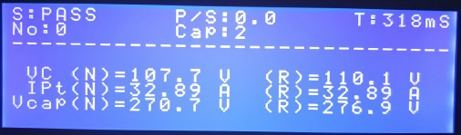
| VC1 | VC2 | VC1 | VC2 | VC1 | VC2 | VC1 | VC2 |
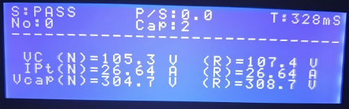
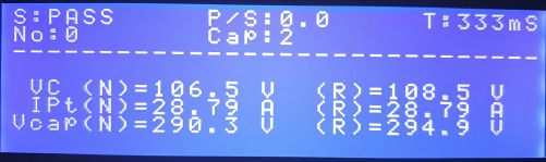
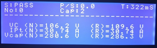
| 105.3V | 109.6V | 106.5V | 108.5V | 106.2V | 109.6V | 107.7V | 110.1V |
| IPP1 | IPP2 | IPP1 | IPP2 | IPP1 | IPP2 | IPP1 | IPP2 |
| 26.64A | 26.64A | 28.79A | 28.79A | 30.74A | 30.74A | 32.89A | 32.89A |
 |
 |
 |
 |
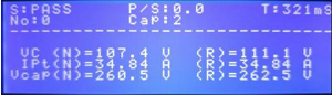
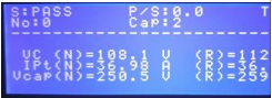
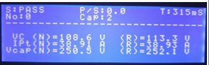
||||
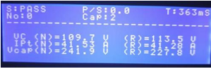
| VC1 | VC2 | VC1 | VC2 | VC1 | VC2 | VC1 | VC2 |
| 107.4V | 111.1V | 108.1V | 112.4V | 108.6V | 113.3V | 109.7V | 113.5V |
| IPP1 | IPP2 | IPP1 | IPP2 | IPP1 | IPP2 | IPP1 | IPP2 |
| 34.84A | 34.84A | 36.98A | 36.90A | 38.91A | 38.93A | 41.53A | 41.28A |
 |
 |
 |
 |
||||
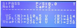
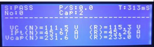
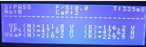
| VC1 | VC2 | VC1 | VC2 | VC1 | VC2 | VC1 | VC2 |
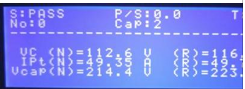
| 110.5V | 114.7V | 111.5V | 115.3V | 111.8V | 116.2V | 112.6V | 116.7V |
| IPP1 | IPP2 | IPP1 | IPP2 | IPP1 | IPP2 | IPP1 | IPP2 |
| 43.58A | 43.36A | 45.67A | 45.26A | 47.69A | 47.63A | 49.35A | 49.75A |
 |
 |
||||||
| VC1 | VC2 | VC1 | VC2 | ||||
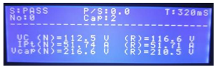
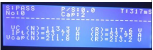
| 112.5V | 116.6V | 113.3V | 117.6V | ||||
| IPP1 | IPP2 | IPP1 | IPP2 | ||||
| 51.74A | 51.71A | 53.73A | 53.95A | ||||
Designed for the "window protection" requirements of 90V bus or power supplies that may reach corresponding voltage levels, as well as 120V withstand voltage power chips, by utilizing a lower surge clamping voltage and a verification method oriented to actual surge waveforms, it helps customers significantly reduce the overvoltage stress and long-term reliability risks of DC-DC chips without major system architecture changes. For bus protection scenarios pursuing "lower clamping voltage and higher system stability," the NR5.0SMDJ90CA can serve as an upgrade option over traditional TVS devices in the same class.
 Hot News


 沪公网安备31011702889749号