
 Global


The sensitivity of gesture recognition modules is both their core advantage and the root of their vulnerability. These modules rely on high-precision optical sensors and high-speed digital interfaces to capture subtle fingertip trajectories. Their internal CMOS sensors and low-voltage logic chips are extremely sensitive to electrostatic discharge (ESD) and electrical overstress (EOS). A seemingly trivial fingertip touch, or moving the module in a dry environment, can generate electrostatic pulses of thousands of volts, which directly break down the sensitive transistors on the I²C or SPI interfaces, leading to abnormal module behavior, data corruption, or even permanent damage. Such failures are often latent, initially appearing as reduced recognition rate or intermittent malfunctions, posing a major hidden risk to product reliability and after-sales support.

First: I²C, UART, and SPI as High-Speed Pathways for ESD Intrusion
The communication interface of a gesture module is its lifeline for interacting with the main controller and is also the most vulnerable path for ESD intrusion. Taking the most mainstream I²C interface as an example, its SDA and SCL lines typically use open-drain or push-pull outputs, directly exposed to the external environment. When a charged human body or equipment contacts the interface header pins, ESD pulses can travel directly along the signal lines to the chip pins. More critically, the multi-device sharing characteristic of the I²C bus means an ESD event at one node may couple through the bus, affecting other innocent devices. UART and SPI interfaces face similar risks, especially in scenarios supporting hot-plugging or connections via ribbon cables, where data lines like TX/RX, MOSI/MISO are highly susceptible to arc discharge during plugging/unplugging.
The core of electrostatic protection for these high-speed data interfaces lies in clamping the high-voltage pulse to a safe level within an extremely short time while not introducing signal integrity issues. Traditional single TVS diodes may degrade high-speed signal edges due to excessive junction capacitance. For this reason, YINT provides an optimized comprehensive solution for signal interface protection in gesture modules. For protecting critical signal interfaces such as I²C, UART, and SPI, it is recommended to use ultra-low capacitance ESD protection devices, such as the ESD5V0D8B or ESD5V0D9B. These devices feature an extremely low load capacitance with a typical value of only 0.5pF, ensuring that signal rise/fall times are almost unaffected even at I²C clock rates of 400kHz or higher. Their bidirectional symmetrical structure can simultaneously protect differential or single-ended signal lines like SDA/SCL, TX/RX, discharging ESD energy exceeding 8kV contact discharge to ground within nanoseconds.
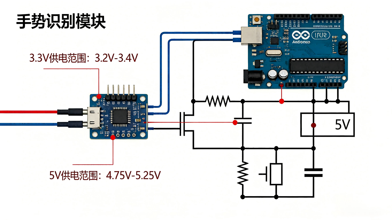
Second: The 3.3V Power Rail
A Non-negligible Secondary Impact Path
Besides direct attacks on signal lines, ESD can also cause damage through the power path. The VCC pin (typically 3.3V) of the gesture module directly supplies power to all core chips. When signal lines suffer an ESD strike, part of the energy can couple to the power rail through the chip's internal circuitry, causing instantaneous voltage spikes on the power supply. This may lead to a complete module logic reset or latch-up. Therefore, deploying a TVS diode specifically for DC power protection near the VCC pin is crucial.
For DC 3.3V power input protection, the ESD3V3D3B is recommended. This is a TVS optimized for 3.3V systems. Its precise breakdown voltage and low clamping voltage (Vc) ensure that overvoltage experienced by downstream circuits during surge events is limited to an absolutely safe range. Using it in conjunction with the ESD5V0D8B on signal lines forms a comprehensive protection network from signals to power, ensuring ESD energy has the lowest impedance path for discharge rather than penetrating the core chips.
Third: Protection Strategy for the INT (Interrupt) Pin
The INT (Interrupt) pin of a gesture module is a special digital output pin used for efficiently notifying the main controller. Although it is an output, in certain circuit layouts, long traces can make it act as a receiving antenna for ESD coupling. The protection for this pin can follow the same principle as for signal lines; selecting the ESD5V0D8B is sufficient. Its fast response time ensures the integrity of the interrupt pulse is not compromised.
Finally: Practical Layout
Integrating Protection Devices into the Design
Effective protection relies not only on selecting the right components but also on correct PCB layout. YINT Electronic's ESD protection devices all use compact packages (e.g., SOD-323, DFN1006), facilitating placement near the entry points of header connectors or board-to-board connectors. The principle of "protection first, filtering second" must be followed: Protection devices (ESD5V0D8B/ESD3V3D3B) should be placed as close as possible to the interface contacts, ensuring ESD current is diverted before entering the internal board circuitry. Filtering beads or capacitors can then be placed afterward as needed. The power protection device ESD3V3D3B should be placed before the power input filter capacitor, ensuring its ground pin is connected to the system's main ground reference plane via the shortest and widest possible path.
For modules using dedicated interfaces such as Gravity and Grove, the protection design should be integrated onto the core board, rather than relying on external sockets. It is recommended to reserve component designators for these protection devices for all external interfaces in the schematic during the initial project design phase and lock their positions during the PCB layout stage. A robust gesture recognition design begins with full respect for and meticulous defense against the "invisible killer" of electrostatic discharge.

 Hot News


 沪公网安备31011702889749号

