Home
CN
Products
EMS Products
TVS Diodes
ESD Protection Diodes
Resettable Fuses
Thyristor Surge Suppressor
Gas Discharge Tubes
Schottky Barrier Diodes
Varistors
NTC thermistors MF72
eFuse
NTC thermistors MF52、MF58
EMI Products
Common Mode Choke
Power Inductors
Ferrite Beads
Common-mode Chokes for CAN FD
Sensors
Temperature sensor devices
Temperature sensor module
Power Devices
MOSFET
Rectifier Diodes
Zener Diodes
Surge Protective Device
SPD for Power Supply
SPD for Signal
SPD for Power + Signal
SCB
Applications
Industrial
Medical & healthcare
Automotive
Energy infrastructure
Consumer electronics
Electronic detonator
Client Cases
Development
Industry Layout
Patent Qualifications
Production Management
Product Planning
Our Future
News & Events
Corporate News
Industry News
Product Knowledge
Training & Education
About
Company Profile
Cultural Philosophy
Organizational Structure
Development History
Sales Network
Honors and Certifications
Contact Us
Support
Sample Request
Technical Support
EMC/CNAS Test
FAQ
Cross-reference search
Careers
Career Development
Employee Culture
Benefits and Compensation
Search jobs
Global
CN
Home
Products
EMS Products
EMI Products
Sensors
Power Devices
Surge Protective Device
Cross-reference search
TVS Diodes
ESD Protection Diodes
Resettable Fuses
Thyristor Surge Suppressor
Gas Discharge Tubes
Schottky Barrier Diodes
Varistors
NTC thermistors MF72
eFuse
NTC thermistors MF52、MF58
Common Mode Choke
Power Inductors
Ferrite Beads
Common-mode Chokes for CAN FD
Temperature sensor devices
Temperature sensor module
MOSFET
Rectifier Diodes
Zener Diodes
SPD for Power Supply
SPD for Signal
SPD for Power + Signal
SCB
Applications
Industrial
Medical & healthcare
Automotive
Energy infrastructure
Consumer electronics
Electronic detonator
Industrial Connectivity and Communication
Industrial automation
Industrial motion and drive
Sensing and Human machine interface (HMI)
Lighting
PLC IoT gateway
Power line Carrier
HMI
PLC
Industrial controller I/O system
Inverter for motion control system
Servo drive for motion controller
Industrial alarm devices
Sensors
Smart lights
Landscape lights
Diabetes healthcare
Hospital patient care
In-vitro diagnostics
Blood glucose monitor
Dental medical equipment
Oxygen concentrator
Blood pressure monitor
Pulsating pulse oximeter
Comprehensive diagnostic and treatment equipment for tinnitus and hearing loss
Infusion pump
Electronic chair
Electronic bed
CPAP ventilator
Electrocardiogram (ECG)
Portable blood coagulation analyzer
Semi-automatic thromboelastography
Immunoassay analyzer
Fecal analyzer
Flow cytometer
Molecular analyzer
Advanced driver assistance systems (ADAS)
Body electronics
Car access & security systems
Car access & security systems
Lighting
Infotainment & cluster
Car entertainment system
Power supply
In-cabin camera module
Mirror replacement/camera mirror system
Front camera
Rear door module
Wiper module
Kick to open module
PEPS
Heat pump module
Interior light
Headlight Adaptive LED Driver Module
Headlight HB/LB LED Driver Module
Small light
Rear light
Zone control module
Domain gateway
Automotive USB charging
Premium audio
Automotive display
Onboard battery charger
12V/48V power distribution box
48V New Energy System
Energy storage systems
Charging pile
Smart meter
Smart circuit breakers
Grid automation
Micro inverter
Uninterruptible power supply
Battery management system (BMS)
DC charging (pile) station
AC charging (pile) station
Gas meter
Electricity meter
Water meter
Smart electrical panel
Solid state circuit breaker (SSCB)
Industrial circuit breaker
GFCI/RCD circuit breaker
DFCI circuit breaker
AFCI circuit breaker
Fault indicator (FI)
Power quality meter
Power quality analyzer
Grid asset monitoring
High-voltage direct current (HVDC) power transmission
Personal computing and entertainment
Smart Home and IoT
Personal travel and drones
Power and charging
VR glasses
Desktop computer
Smart parcel lockers
Smart lock
Two-wheeled vehicle tracker
E-BIKE
Drone
PD
Electronic detonator
Electronic detonator
Support
Support
With over a thousand cooperative customers and 17 years of service experience, we can provide you with everything from model selection to technical support
Sample Request
Technical Support
EMC/CNAS Test
FAQ
Cross-reference search
Development
Development
Our unyielding mission is to continuously innovate and lead the industry's progress.
Industry Layout
Patent Qualifications
Production Management
Product Planning
Our Future
News & Events
News & Events
We will share every little bit of our life with you at all times
Corporate News
Industry News
Product Knowledge
Training & Education
About
About
Yinte Electronics integrates technology research and development, chip manufacturing, packaging and testing, sales, and service
Company Profile
Cultural Philosophy
Organizational Structure
Development History
Sales Network
Honors and Certifications
Client Cases
Contact Us
Careers
Careers
Unleash potential together, shape a healthy future for humanity
Career Development
Employee Culture
Benefits and Compensation
Search jobs
Select model to search
|
Cross-reference search
Online Message
Name
*
Company
Email
*
Phone
Message
Contact
News & Events
We will share every little bit of our life with you at all times
Corporate News
Industry News
Product Knowledge
Training & Education
News & Events
We will share every little bit of our life with you at all times
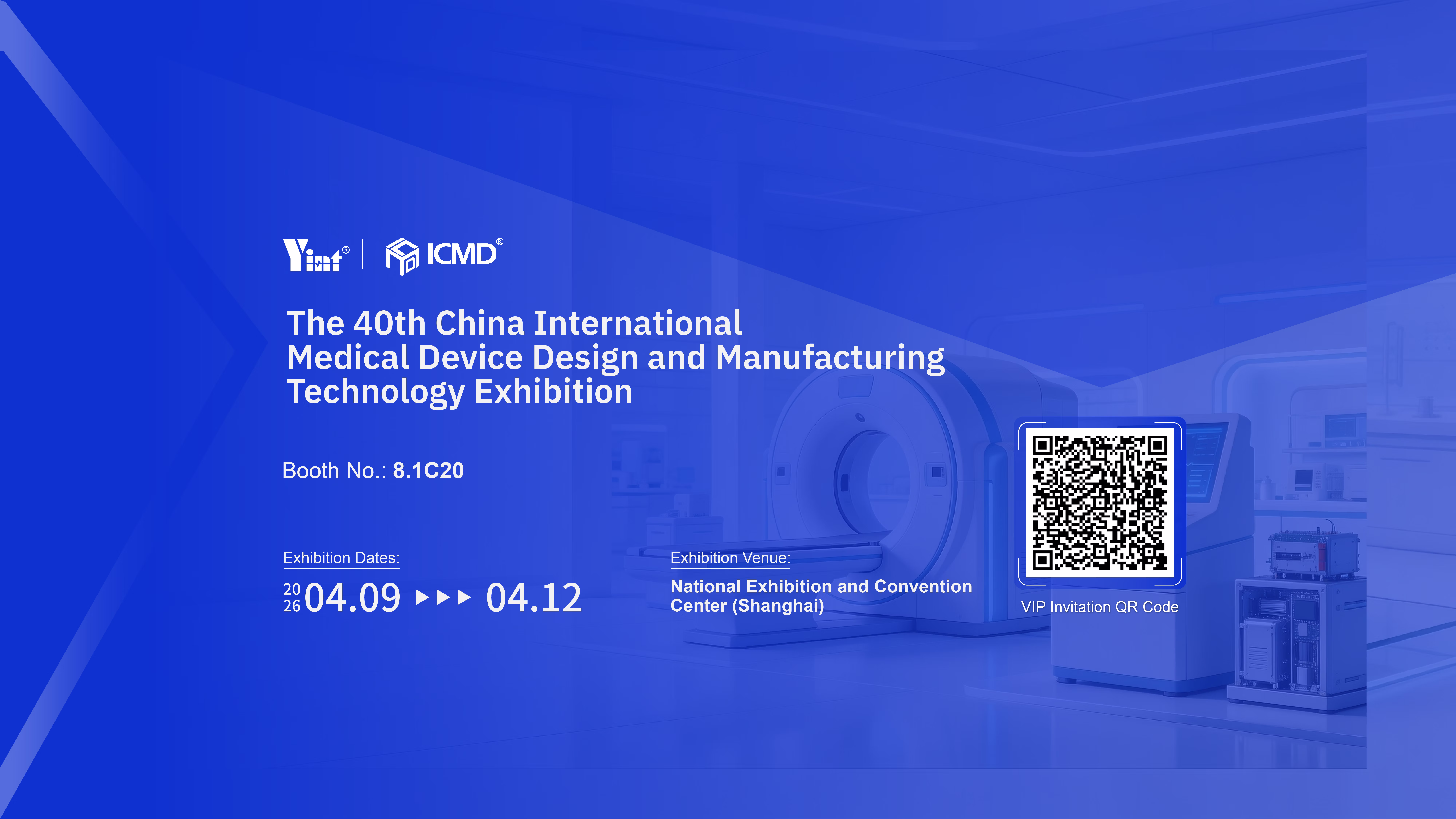
YINT Electronics at ICMD 2026 | Medical Protection Solutions
2026-04-03
Join YINT Electronics at the 40th China International Medical Device Design & Manufacturing Exhibition (ICMD 2026). Discover advanced EMC, ESD, and surge protection solutions for medical applications.
Explore More
ESD Diode Terminology in Multiple Languages
2025-12-06
Clamp voltage
Wiring layout
ESD diode
Surge protection device
Protective device
Response time
Core Parameters of ESD Diodes
2025-12-06
ESD Diodes: The Invisible Guardians of Electronic Devices. In today’s increasingly precise electronic devices, electrostatic discharge (ESD) has become a major threat to circuit reliability. A tiny static pulse is enough to damage fragile integrated circuits. ESD diodes, as specialized semiconductor devices for electrostatic protection, provide a low-impedance discharge path on sensitive signal lines or power lines, safely dissipating dangerous ESD energy to the ground, thereby protecting the core chips. Understanding their core parameters is key to proper selection and application. In-Depth Analysis of Five Core Parameters. Choosing a suitable ESD diode...
ESD Electrostatic Diode Chip Dicing Depth and Speed
2025-12-06
Exploring ESD Electrostatic Diodes: The Art of Balancing Depth and Speed in Chip Dicing Process. In the back-end process of semiconductor manufacturing, chip dicing is a critical step in cutting wafers into individual chips. For devices like ESD (Electrostatic Discharge) protection diodes, which have extremely high requirements for performance and reliability, parameter control in the dicing process, especially dicing depth and speed, directly affects the final product quality, yield, and even service life. This is not just simple cutting, but a precise balancing art. Dicing Depth: Ensuring Separation and Protecting Structural Balance. Dicing depth mainly refers to the cutting blade penetrating the wafer...
Deepening Industry-Academia-Research Integration: Shanghai University of Engineering Science Faculty and Students Visit Inte Electron, Exploring New Applications in Materials Science
2025-11-29
Deepen the integration of industry and education, break down the wall between theoretical teaching in universities and practical application in enterprises, and enable future engineers to have zero distance exposure to cutting-edge technologies in the electronic components industry
Vehicle Ethernet Standard Architecture
2025-11-29
OPEN Alliance was established in 2011, focusing on the standardization of automotive Ethernet CML3225A-201T for common mode inductors
Forward Conduction Voltage VF and ESD's VBR_forward
2025-11-27
What is the difference between the forward conduction voltage VF of ordinary diodes and the forward breakdown voltage VBR_forward of ESD protection diodes?
First: Ordinary diode VF: The threshold voltage for PN junction conduction under forward bias (silicon diode ≈0.7V). After conduction, current increases slowly with voltage, no "breakdown" characteristic. Damage occurs when forward current is excessive due to thermal dissipation
ESD tube VBR_forward: The voltage at which avalanche breakdown occurs under forward bias. After breakdown, current surges sharply (e.g., when VBR_forward=6V)
The latest developments in SENT protocol
2025-11-27
The protocol is a digital communication standard designed specifically for point-to-point data transmission between sensors and ECU (Electronic Control Unit) in the field of automotive electronics. Its full name is the Single Edge Nibble Transmission protocol The core specification is based on SAE J2716 (the latest version being SAE J2716-201604 released in 2016) and is one of the key technologies for digital transmission of sensors in modern automobiles 1. The application scope continues to expand Global SENT Protocol Transmission by 2025
How is the "Dynamic Resistance (Rd)" of ESD Protection Diodes Defined?
2025-11-21
Humanoid robot BMS electrostatic protection, humanoid robot sensor module electrostatic protection, humanoid robot position sensor electrostatic protection, humanoid robot motor driver electrostatic protection, humanoid robot system controller electrostatic protection, lawn mower robot electrostatic protection, floor cleaning robot electrostatic protection, robot CPU and computing board electrostatic protection, robot I/O module electrostatic protection,
Robot sensor module electrostatic protection, robot servo driver electrostatic protection, robot position sensor electrostatic protection, robot position feedback aggregator electrostatic protection, robot safety module electrostatic protection, robot teach pendant (HMI) electrostatic protection,
Robot communication module electrostatic protection, mobile robot BMS electrostatic protection, mobile robot CPU and computing module electrostatic protection, mobile robot sensor electrostatic protection, mobile robot safety module electrostatic protection, mobile robot motor control electrostatic protection, mobile robot communication module electrostatic protection
Why Do Some ESD Protection Diodes Use "Bidirectional Breakdown" Design?
2025-11-15
USB 2.0/3.0, HDMI, DP, Ethernet (RJ45), I2C/SPI bus (bidirectional communication), DC-DC power input ports, battery power supply lines, 5V/12V device power interfaces
总计 407
1
2
...
10
11
12
13
14
15
16
...
45
46

 Global


 沪公网安备31011702889749号
