
 Global


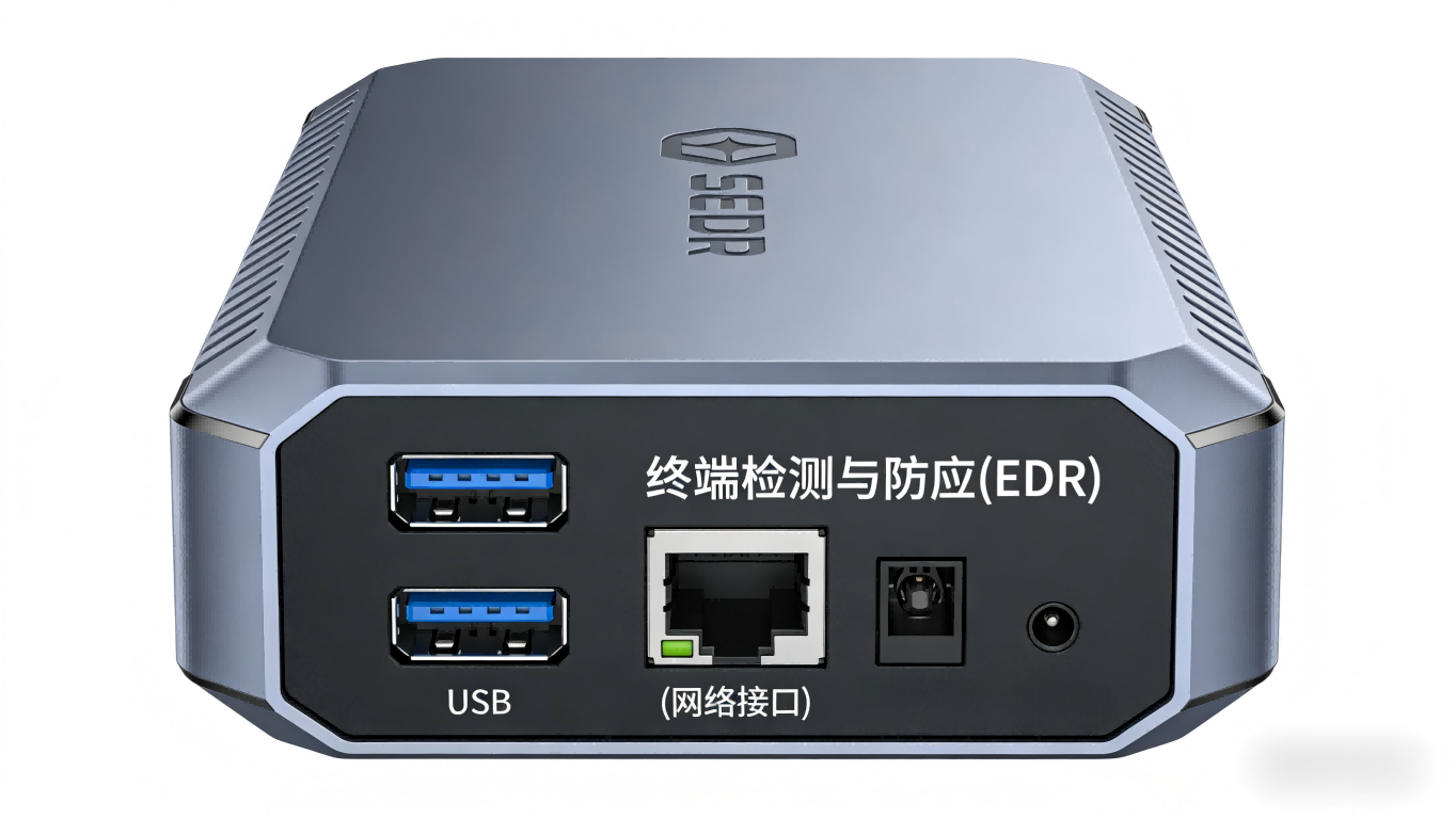
At the core of data centers and computing power networks, switches are not only the hubs for data flow but also the cornerstone of the entire system's stability. As data rates evolve towards 400G/800G and beyond, the high-speed SerDes, DDR memory, clock networks, and various management interfaces within switches face unprecedented electromagnetic compatibility (EMC) challenges. Particularly for hardware EDR (Endpoint Detection and Response) dedicated terminals, which serve as the security perimeter, they integrate complex network processing, security chips, and multiple types of industrial interfaces. Achieving high-intensity data processing and withstanding harsh industrial environments within a compact space imposes extreme "both/and" requirements on EMC design—it must ensure its own high-speed signal integrity (EMI) while also resisting various electromagnetic disturbances (EMS) from the external power grid and interface coupling. Any oversight in either aspect can lead to packet errors, system crashes, or even hardware damage, the cost of which is catastrophic in 7x24-hour non-stop data centers.
Strategy 1: Analyzing the EMC Risk Matrix of Hardware EDR Terminals
Hardware EDR terminals are essentially highly integrated, specialized industrial computers. Their EMC risks do not exist in isolation; rather, they form a three-dimensional risk matrix based on functional modules and interface types.
Core Risk One: "Self-Interference" and "External Interference" from High-Speed Data and Network Interfaces
This is the most critical challenge. Gigabit/10-Gigabit Ethernet PHY chips, DDR memory buses, and potential PCIe channels within the device generate rich high-frequency harmonic noise during operation. If this noise couples through space radiation or the power/ground plane, it can interfere with the device's own sensitive RF receiving circuits (e.g., optional 4G/5G modules) or adjacent boards, constituting an EMI problem. Simultaneously, all external physical interfaces—RJ45, SFP optical module cages, USB, Console ports—are "gateways" for the intrusion of external electrostatic discharge (ESD), electrical fast transient (EFT) bursts, and surge. A single electrostatic discharge generated by an operator hot-plugging a network cable, or a surge coupled onto a network cable due to a remote lightning strike, can travel along the link and directly strike the PHY chip, causing port failure.
Core Risk Two: "Violent" Transients Introduced by Industrial Field Interfaces
The RS232/RS485 serial ports and DI/DO digital I/O interfaces designed for hardware EDRs to integrate into industrial environments are key differentiators from ordinary IT equipment and are also the hardest-hit areas for EMS risks. These long-line interfaces are highly susceptible to coupling extremely high-energy surges and EFTs generated by on-site relays, motor start/stops, and inverter operations. For example, an RS485 bus in a factory environment may need to withstand surge impacts of ±2kV or even ±4kV as defined by the IEC 61000-4-5 standard. Its energy level is far beyond that of data ports, requiring dedicated high-energy-capacity protection solutions.
Core Risk Three:
Hardware EDR supports a wide DC input voltage range of 9V-60V and may be compatible with 110V/220V AC. Its internal Power Management IC (PMIC) requires multi-stage DC-DC conversion to provide various voltages such as 1.0V, 1.8V, and 3.3V for the CPU, memory, and chipset. This complex power network is both the primary source of internal switching noise (e.g., dV/dt from Buck converters) and the propagation path for external conducted disturbances (e.g., grid fluctuations, EFT injected via the power line). Noise in the power network directly elevates ground potential, degrading the reference ground for all analog and digital circuits, leading to system logic errors or performance degradation.
Strategy 2: Constructing a Hierarchical, Full-Link EMC Protection Architecture
In response to the aforementioned risk matrix, fragmented, post-hoc patchwork protection designs are no longer adequate. It is essential to construct a hierarchical, full-link EMC protection system for hardware EDR terminals at the architectural level, to "keep interference out" and "dissipate noise within."
First Level: Port-Level Precision Protection
Port-level precision protection involves equipping each data channel with a "dedicated guard." This is the first and most critical physical line of defense in the protection system. Its core principle is "prescribing the right remedy for the illness," selecting the most appropriate combination of EMI filtering and EMS protection devices based on the interface's signal rate, operating voltage, and potential threat level.
Gigabit/10-Gigabit Ethernet Electrical Port (RJ45) Protection: This is the main data highway. For Gigabit (1G) Ethernet, both signal integrity and surge/ESD protection must be addressed simultaneously. It is recommended to use a CMZ2012A-900T common mode choke on the PHY chip side, close to the connector. This component maintains excellent common-mode noise suppression capability at frequencies up to 100 MHz and above, effectively filtering common-mode interference on signal lines and improving signal quality. On the EMS protection side, it is essential to select a TVS array with low capacitance and fast response speed to protect the PHY chip. ESDLC3V3D3B or ESD0524P are ideal choices, with junction capacitance as low as a typical 0.5pF, ensuring minimal impact on high-speed differential signals while rapidly clamping ±30kV contact discharge ESD and common surge overvoltages.
Industrial Serial Bus (RS232/RS485) Protection: These interfaces have relatively low speeds but face high-energy threats. The focus of protection is on energy dissipation. In addition to using CMZ2012A-900T for necessary filtering, for RS485 buses, it is recommended to use the ESDSM712 integrated bus protection chip, or to combine SMBJ6.5CA TVS diodes with gas discharge tubes to form a three-stage protection circuit, robustly handling surge impacts above ±4kV. For RS232 interfaces, devices such as ESD15VAPB and SM18CA can be selected for protection.
USB/Console and Other Medium/Low-Speed Data Interface Protection: USB 2.0/3.0 and debug console ports also require low-capacitance protection. Mature chipset solutions are provided for such universal data interfaces. For example, using CMZ2012A-900T to filter noise, combined with multi-channel TVS arrays like ESDLC5V0D8B, ESDSRVLC05-4, or ESD0524P to provide integrated, compact ESD protection for multiple data lines.
Second Level: Board-Level Power Network Purification
Board-level power network purification involves creating a clean "energy lineage." A "quiet" power supply is the foundation of system stability. The protection strategy must be implemented step-by-step from input to load.
2.1 Input Stage Coarse Protection and Filtering
At the wide-voltage DC input port (e.g., 24V DC), a TVS diode with high surge current capability should be placed first to absorb high-energy surges from the power line. For instance, for a 24V system, the SMDJ24CA can be selected. Following this, a high-current power inductor, such as the CMZ7060A-701T, should be deployed to form an input LC filter network, effectively suppressing low-frequency conducted noise.
2.2 High-Frequency Noise Suppression at the DC-DC Converter Stage: The input and output terminals of each switching power converter (e.g., Buck circuits converting 24V to 5V, 5V to 3.3V) are sources of high-frequency switching noise. Ferrite beads or small-sized power inductors, such as corresponding models from the CML or CMZ series, must be placed near the input capacitors to filter out the switching frequency and its harmonics. Simultaneously, corresponding voltage clamping protection devices should be provided for each low-voltage DC bus (e.g., 3.3V, 5V). For example, for a 5V bus, select ESD5V0D3B or SMBJ6.0CA to clamp transient overvoltages caused by load transients or coupling.
Third Level:
System-Level Grounding and Shielding — Establishing a Unified "Electromagnetic Order". Even the best components rely on good PCB design and system architecture. A complete ground plane must be used to provide a low-impedance discharge path for all protection devices. Reasonable partitioning and layout should be implemented for high-speed digital areas, analog areas, power supply areas, and interface areas. For critical high-speed signal lines, differential routing with ground shielding should be employed. The metal enclosure of the hardware EDR should be properly grounded, and conductive gaskets or foam should be used at openings such as Ethernet ports and serial ports to ensure shielding continuity.
Strategy 3: EMI + EMS Complete Solution Selection Guide
Based on the aforementioned architecture, we have compiled a complete set of recommended component solutions for the key sections of the hardware EDR terminal to facilitate a successful first-pass design.
| Gigabit Ethernet Port | Radiated Interference, ESD, Surge | CMZ2012A-900T (Common Mode Choke) | ESDLC3V3D3B or ESD0524P (Low Capacitance TVS Array) | Ensures signal integrity, protects against interface electrostatic discharge and surge, meeting IEC 61000-4-2/5 Level 4 requirements |
| RS485 Industrial Bus | High-Energy Surge, EFT, Common-Mode Interference | CMZ2012A-900T (Common Mode Choke) | ESDSM712 (Integrated Protection) or SMBJ6.5CA + GDT (Discrete Protection) | Provides high-reliability, high-energy-capacity protection for long-line industrial communication, suitable for harsh electromagnetic environments |
| USB 3.0/2.0 Data Port | ESD, Data Line Noise | CMZ2012A-900T (Common Mode Choke) | ESDLC5V0D8B or ESDSRVLC05-4 (Multi-Channel TVS) | Ultra-low capacitance ensures no distortion of high-speed USB signals; integrated package saves board space |
| 24V DC Wide-Voltage Input | Power Line Surge, Conducted Noise | CMZ7060A-701T (Power Inductor) | SMDJ24CA (TVS) | Constructs primary protection and filtering at the power entry point, providing clean and stable input for subsequent circuits |
| Internal 5V Power Rail | Load Dump, Switching Noise, Coupled Overvoltage | Select CML/CMZ series ferrite beads/inductors based on current | ESD5V0D3B or SMBJ6.0CA (TVS) | Protects core chip power pins, preventing logic errors or latch-up effects caused by voltage transients |
Strategy 4: Closed-Loop Strategy from Design to Verification
Excellent EMC design is a closed-loop process. During the early schematic and PCB design stages, the aforementioned protective devices and layout considerations should be incorporated as constraints. It is recommended that, even if the initial design assessment indicates low risk, footprint positions for protective devices and necessary discharge grounding vias be reserved on critical interfaces and power paths.
During the prototype testing phase, comprehensive EMC pre-compliance testing must be conducted, with a focus on:
Radiated Emissions (RE): Verify the effectiveness of noise suppression for internal high-speed circuits and switching power supplies.
Electrostatic Discharge Immunity (ESD): Perform contact discharge and air discharge tests on all user-accessible interfaces.
Surge and EFT Immunity: Apply standard surge and burst pulses to power ports and industrial ports (e.g., RS485) to verify the durability of the protection circuitry.
Summary:
When test issues arise, first check if the selection of protective devices is appropriate (e.g., whether the TVS clamping voltage is sufficiently low and its power rating is sufficiently high). Next, inspect their PCB layout (whether the return path is short and wide, and whether the signal passes through the protective device before reaching the chip). The complete solution provided here features device parameters that have been rigorously matched and extensively field-validated, significantly shortening customers' debugging cycles and improving the success rate of passing EMC certification on the first attempt.
For high-density, high-reliability equipment such as data center switches and hardware EDR terminals, EMC has evolved from a "compliance item" to a "core competitive advantage." Adopting a full-link EMI+EMS solution—from ports to power supplies, from filtering to protection—is not only a technical approach to solving electromagnetic compatibility challenges but also a solid foundation for building long-term product reliability and superior quality. It is recommended that hardware engineers directly include the aforementioned recommended device combinations in the Bill of Materials (BOM) at the project initiation stage, safeguarding the stable operation of the product from the very source.
 Hot News


 沪公网安备31011702889749号

