Global
EN
Applications
Support
Support
With over a thousand cooperative customers and 17 years of service experience, we can provide you with everything from model selection to technical support
Development
Development
Our unyielding mission is to continuously innovate and lead the industry's progress.
News & Events
News & Events
We will share every little bit of our life with you at all times
About
About
Yinte Electronics integrates technology research and development, chip manufacturing, packaging and testing, sales, and service
Careers
Careers
Unleash potential together, shape a healthy future for humanity
News & Events
We will share every little bit of our life with you at all times
Corporate News Industry News Product Knowledge Downloads

What is a Silicon Semiconductor PN Junction?

Source:Yint Time:2023-06-17 Views:2939
Share:

In silicon semiconductors, PN typically refers to the "Positive-Negative" structure, which is the junction between the positive region (P-region) and the negative region (N-region). Positive                     Negative


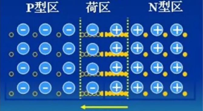
This structure is formed by p-type (positive-type) and n-type (negative-type) semiconductor materials. In this structure, the doping in the P-type semiconductor region contains positive ions (such as boron), while the doping in the N-type semiconductor region contains negative ions (such as phosphorus or arsenic). The English abbreviation for this structure is PN junction.


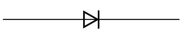
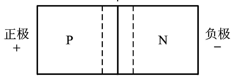
Note that PN here refers to the structure, not the abbreviated meaning of PN.