Home
CN
Products
EMS Products
TVS Diodes
ESD Protection Diodes
Resettable Fuses
Thyristor Surge Suppressor
Gas Discharge Tubes
Schottky Barrier Diodes
Varistors
NTC thermistors MF72
eFuse
NTC thermistors MF52、MF58
EMI Products
Common Mode Choke
Power Inductors
Ferrite Beads
Common-mode Chokes for CAN FD
Sensors
Temperature sensor devices
Temperature sensor module
Power Devices
MOSFET
Rectifier Diodes
Zener Diodes
Surge Protective Device
SPD for Power Supply
SPD for Signal
SPD for Power + Signal
SCB
Applications
Industrial
Medical & healthcare
Automotive
Energy infrastructure
Consumer electronics
Electronic detonator
Client Cases
Development
Industry Layout
Patent Qualifications
Production Management
Product Planning
Our Future
News & Events
Corporate News
Industry News
Product Knowledge
Training & Education
About
Company Profile
Cultural Philosophy
Organizational Structure
Development History
Sales Network
Honors and Certifications
Contact Us
Support
Sample Request
Technical Support
EMC/CNAS Test
FAQ
Cross-reference search
Careers
Career Development
Employee Culture
Benefits and Compensation
Search jobs
Global
CN
Home
Products
EMS Products
EMI Products
Sensors
Power Devices
Surge Protective Device
Cross-reference search
TVS Diodes
ESD Protection Diodes
Resettable Fuses
Thyristor Surge Suppressor
Gas Discharge Tubes
Schottky Barrier Diodes
Varistors
NTC thermistors MF72
eFuse
NTC thermistors MF52、MF58
Common Mode Choke
Power Inductors
Ferrite Beads
Common-mode Chokes for CAN FD
Temperature sensor devices
Temperature sensor module
MOSFET
Rectifier Diodes
Zener Diodes
SPD for Power Supply
SPD for Signal
SPD for Power + Signal
SCB
Applications
Industrial
Medical & healthcare
Automotive
Energy infrastructure
Consumer electronics
Electronic detonator
Industrial Connectivity and Communication
Industrial automation
Industrial motion and drive
Sensing and Human machine interface (HMI)
Lighting
PLC IoT gateway
Power line Carrier
HMI
PLC
Industrial controller I/O system
Inverter for motion control system
Servo drive for motion controller
Industrial alarm devices
Sensors
Smart lights
Landscape lights
Diabetes healthcare
Hospital patient care
In-vitro diagnostics
Blood glucose monitor
Dental medical equipment
Oxygen concentrator
Blood pressure monitor
Pulsating pulse oximeter
Comprehensive diagnostic and treatment equipment for tinnitus and hearing loss
Infusion pump
Electronic chair
Electronic bed
CPAP ventilator
Electrocardiogram (ECG)
Portable blood coagulation analyzer
Semi-automatic thromboelastography
Immunoassay analyzer
Fecal analyzer
Flow cytometer
Molecular analyzer
Advanced driver assistance systems (ADAS)
Body electronics
Car access & security systems
Car access & security systems
Lighting
Infotainment & cluster
Car entertainment system
Power supply
In-cabin camera module
Mirror replacement/camera mirror system
Front camera
Rear door module
Wiper module
Kick to open module
PEPS
Heat pump module
Interior light
Headlight Adaptive LED Driver Module
Headlight HB/LB LED Driver Module
Small light
Rear light
Zone control module
Domain gateway
Automotive USB charging
Premium audio
Automotive display
Onboard battery charger
12V/48V power distribution box
48V New Energy System
Energy storage systems
Charging pile
Smart meter
Smart circuit breakers
Grid automation
Micro inverter
Uninterruptible power supply
Battery management system (BMS)
DC charging (pile) station
AC charging (pile) station
Gas meter
Electricity meter
Water meter
Smart electrical panel
Solid state circuit breaker (SSCB)
Industrial circuit breaker
GFCI/RCD circuit breaker
DFCI circuit breaker
AFCI circuit breaker
Fault indicator (FI)
Power quality meter
Power quality analyzer
Grid asset monitoring
High-voltage direct current (HVDC) power transmission
Personal computing and entertainment
Smart Home and IoT
Personal travel and drones
Power and charging
VR glasses
Desktop computer
Smart parcel lockers
Smart lock
Two-wheeled vehicle tracker
E-BIKE
Drone
PD
Electronic detonator
Electronic detonator
Support
Support
With over a thousand cooperative customers and 17 years of service experience, we can provide you with everything from model selection to technical support
Sample Request
Technical Support
EMC/CNAS Test
FAQ
Cross-reference search
Development
Development
Our unyielding mission is to continuously innovate and lead the industry's progress.
Industry Layout
Patent Qualifications
Production Management
Product Planning
Our Future
News & Events
News & Events
We will share every little bit of our life with you at all times
Corporate News
Industry News
Product Knowledge
Training & Education
About
About
Yinte Electronics integrates technology research and development, chip manufacturing, packaging and testing, sales, and service
Company Profile
Cultural Philosophy
Organizational Structure
Development History
Sales Network
Honors and Certifications
Client Cases
Contact Us
Careers
Careers
Unleash potential together, shape a healthy future for humanity
Career Development
Employee Culture
Benefits and Compensation
Search jobs
Select model to search
|
Cross-reference search
Online Message
Name
*
Company
Email
*
Phone
Message
Contact
News & Events
We will share every little bit of our life with you at all times
Corporate News
Industry News
Product Knowledge
Training & Education
News & Events
We will share every little bit of our life with you at all times
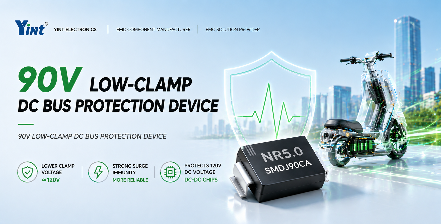
90V DC Bus Low-Clamping TVS Surge Protection Solution|120V Withstand DC
2026-05-14
NR5.0SMDJ90CA low clamping TVS diode protects 90V bus systems, clamping surges near 120V to prevent DC-DC chip breakdown and latent failure.
Explore More
Huawei's first overseas factory will land in France
2023-12-12
According to China Times News on December 10th, Zhang Minggang, Deputy General Manager of Huawei France, revealed that Huawei's first overseas factory has been confirmed to be located in France, covering an area of about 8 hectares, and is expected to start production by the end of 2025. According to reports, Huawei's project is expected to invest 200 million euros, with an annual output value of up to 1 billion euros. This factory is expected to produce 1 billion units of equipment annually, but not smartphones, but rather chipsets, motherboards, and other components required for 4G and 5G base stations, which can supply the entire European market. According to reports, Huawei entered France in 2003 and currently has 6 research and development centers and 1 global design center in Paris. Huawei announced in 2019 that it would set up a factory in France, originally planned to start production in early 2023, but due to various environmental reasons, it was delayed for a long time.
Semiconductors Needed for Automobiles
2023-12-05
Source: High Chip Circle
Not only for EVs and hybrid vehicles, but also for pure fuel vehicles, semiconductors are essential components. This is a fact that people have witnessed.
Take recent clean diesel vehicles (Clean Diesel Vehicle) as an example, their mode is as follows: each combustion cycle injects fuel about five times, effectively using fuel, extracting torque, although fuel consumption increases, but can discharge clean gas as much as possible.
Although controlled in milliseconds, for computers...
Is the chip industry approaching a turning point in 2024?
2023-12-05
Source: Global Semiconductor Watch On November 28th, the World Semiconductor Trade Statistics Organization (WSTS) released its latest forecast for the semiconductor market. Due to the widespread adoption of generative AI and the rapid increase in demand for related semiconductor products, as well as the expected significant recovery in storage demand, the estimated global semiconductor sales for 2024 have been revised upwards from the previous estimate of $575.997 billion on June 6 to $588.364 billion, an annual increase of 13.1%, surpassing the historical high of $574.084 billion in 2022.
What signals do the latest financial reports of the world's top five storage plants release?
2023-11-16
Source: Sina Weibo, Global Semiconductor Observer Due to the decline in demand, the memory market is under pressure from oversupply and price decline in 2023. However, with the arrival of the fourth quarter, the prices of storage chip products are gradually rising, and the storage chip market is expected to overcome the trough. The latest financial reports of the world's top five original manufacturers also confirm the above viewpoint.
Great Wall Motors' self-developed IGBT mass production and installation
2023-11-16
On November 14th, Great Wall Motors announced that the IGBT independently developed and produced by Xindong Semiconductor, a subsidiary of Great Wall Holdings, has achieved mass production and installation. The project took only 14 months from project initiation and development to installation. At present, the construction of Xindong Semiconductor Wuxi factory has been completed. Since the foundation was laid in February this year, it has taken 8 months for the main body of the factory to be capped, and the first module production line was successfully put into operation on October 28th. The factory has a first-class testing environment in China, which can meet the strict quality management requirements of IGBT power modules, quickly respond to vehicle requirements, and develop products in a targeted manner. In addition, it is reported that in October this year, Great Wall Motors sold 131300 vehicles, a year-on-year increase of 31.04%. The cumulative sales for this year reached 995400 vehicles, a year-on-year increase of 10.29%. Among them, Euler brand cars sold 10800 units in October, a year-on-year increase of 94.29%; The sales of new energy vehicles reached 30551 units, with a cumulative sales of 200897 units from January to October.
Will smartphone RAM jump from 20GB in 2024?
2023-11-16
Source: Science and Technology News Recently, foreign media Wccftech reported that one of the popular trends for 2024 is terminal AI, which is now built into multiple chipsets such as Snapdragon 8 Gen 3, Dimensity 9300, and Exynos2400. There is new news suggesting that smartphones with AI capabilities require more memory, and Android phones with built-in AI capabilities will have a minimum memory capacity of 20GB RAM as the standard. Although 8GB RAM is still the standard for Android smartphones, it has been seen that phones with higher memory than most laptops or PCs have not yet become standard. In order to ensure the smooth execution of AI imaging functions on future devices, Android phones require at least 12GB of RAM, as AI applications and other functions require over 20GB of RAM to operate smoothly. There have been smartphones with over 20GB RAM in the market, and OnePlus has also released high-capacity memory devices, but at that time there was no AI function. If we expect AI functionality to run smoothly, smartphones in 2024 will require higher RAM. It is not yet certain that all Android phone manufacturers will follow suit, considering that multiple Android phone manufacturers are continuously investing in AI, AI will become a key focus for devices in 2024. Therefore, the industry believes that with higher RAM requirements, hardware specifications are more important for modern AI devices than ever before.
What are Power Semiconductor Devices
2023-11-16
Power semiconductor devices refer to electronic devices that can directly achieve electrical energy conversion or circuit control in main circuits, mainly used for power conversion, including rectification, inversion, DC chopping, as well as AC power control, frequency conversion, or phase change. Unlike other types of semiconductors, power semiconductors can withstand high voltage and large current, usually operating in switching state, and are the core of electrical energy conversion and circuit control, playing a key role in efficient generation, transmission, conversion, storage, and control of electrical energy.
Power semiconductor devices can be divided into bipolar power semiconductors and unipolar power semiconductor devices according to carrier type. Bipolar power semiconductor devices include...
Yinte Electronics and Zhenggui Electric have established a strategic partnership
2023-11-16
Recently, Yinte Electronics and Zhenggui Electric have forged a deep strategic partnership. This strategic collaboration is based on the spirit of "mutual benefit, mutual advantage, stability, longevity, efficiency, and quality". Its primary objectives are to enhance overall operational efficiency, reduce operational costs, and improve product and service quality. The aim is to achieve future market expansion strategies for both parties, gain market share, and create greater business value for both parties.
Semiconductor Basic Knowledge
2023-11-09
01
What is a Semiconductor?
"Semiconductor" is a substance whose characteristics are between "conductor" and "insulator", the former conducting electricity like metal, the latter almost not conducting electricity. The ease of current flow is related to the electrical...
总计 444
1
2
...
27
28
29
30
31
32
33
...
49
50

 Global


 沪公网安备31011702889749号
