Home
CN
Products
EMS Products
TVS Diodes
ESD Protection Diodes
Resettable Fuses
Thyristor Surge Suppressor
Gas Discharge Tubes
Schottky Barrier Diodes
Varistors
NTC thermistors MF72
eFuse
NTC thermistors MF52、MF58
EMI Products
Common Mode Choke
Power Inductors
Ferrite Beads
Common-mode Chokes for CAN FD
Sensors
Temperature sensor devices
Temperature sensor module
Power Devices
MOSFET
Rectifier Diodes
Zener Diodes
Surge Protective Device
SPD for Power Supply
SPD for Signal
SPD for Power + Signal
SCB
Applications
Industrial
Medical & healthcare
Automotive
Energy infrastructure
Consumer electronics
Electronic detonator
Client Cases
Development
Industry Layout
Patent Qualifications
Production Management
Product Planning
Our Future
News & Events
Corporate News
Industry News
Product Knowledge
Training & Education
About
Company Profile
Cultural Philosophy
Organizational Structure
Development History
Sales Network
Honors and Certifications
Contact Us
Support
Sample Request
Technical Support
EMC/CNAS Test
FAQ
Cross-reference search
Careers
Career Development
Employee Culture
Benefits and Compensation
Search jobs
Global
CN
Home
Products
EMS Products
EMI Products
Sensors
Power Devices
Surge Protective Device
Cross-reference search
TVS Diodes
ESD Protection Diodes
Resettable Fuses
Thyristor Surge Suppressor
Gas Discharge Tubes
Schottky Barrier Diodes
Varistors
NTC thermistors MF72
eFuse
NTC thermistors MF52、MF58
Common Mode Choke
Power Inductors
Ferrite Beads
Common-mode Chokes for CAN FD
Temperature sensor devices
Temperature sensor module
MOSFET
Rectifier Diodes
Zener Diodes
SPD for Power Supply
SPD for Signal
SPD for Power + Signal
SCB
Applications
Industrial
Medical & healthcare
Automotive
Energy infrastructure
Consumer electronics
Electronic detonator
Industrial Connectivity and Communication
Industrial automation
Industrial motion and drive
Sensing and Human machine interface (HMI)
Lighting
PLC IoT gateway
Power line Carrier
HMI
PLC
Industrial controller I/O system
Inverter for motion control system
Servo drive for motion controller
Industrial alarm devices
Sensors
Smart lights
Landscape lights
Diabetes healthcare
Hospital patient care
In-vitro diagnostics
Blood glucose monitor
Dental medical equipment
Oxygen concentrator
Blood pressure monitor
Pulsating pulse oximeter
Comprehensive diagnostic and treatment equipment for tinnitus and hearing loss
Infusion pump
Electronic chair
Electronic bed
CPAP ventilator
Electrocardiogram (ECG)
Portable blood coagulation analyzer
Semi-automatic thromboelastography
Immunoassay analyzer
Fecal analyzer
Flow cytometer
Molecular analyzer
Advanced driver assistance systems (ADAS)
Body electronics
Car access & security systems
Car access & security systems
Lighting
Infotainment & cluster
Car entertainment system
Power supply
In-cabin camera module
Mirror replacement/camera mirror system
Front camera
Rear door module
Wiper module
Kick to open module
PEPS
Heat pump module
Interior light
Headlight Adaptive LED Driver Module
Headlight HB/LB LED Driver Module
Small light
Rear light
Zone control module
Domain gateway
Automotive USB charging
Premium audio
Automotive display
Onboard battery charger
12V/48V power distribution box
48V New Energy System
Energy storage systems
Charging pile
Smart meter
Smart circuit breakers
Grid automation
Micro inverter
Uninterruptible power supply
Battery management system (BMS)
DC charging (pile) station
AC charging (pile) station
Gas meter
Electricity meter
Water meter
Smart electrical panel
Solid state circuit breaker (SSCB)
Industrial circuit breaker
GFCI/RCD circuit breaker
DFCI circuit breaker
AFCI circuit breaker
Fault indicator (FI)
Power quality meter
Power quality analyzer
Grid asset monitoring
High-voltage direct current (HVDC) power transmission
Personal computing and entertainment
Smart Home and IoT
Personal travel and drones
Power and charging
VR glasses
Desktop computer
Smart parcel lockers
Smart lock
Two-wheeled vehicle tracker
E-BIKE
Drone
PD
Electronic detonator
Electronic detonator
Support
Support
With over a thousand cooperative customers and 17 years of service experience, we can provide you with everything from model selection to technical support
Sample Request
Technical Support
EMC/CNAS Test
FAQ
Cross-reference search
Development
Development
Our unyielding mission is to continuously innovate and lead the industry's progress.
Industry Layout
Patent Qualifications
Production Management
Product Planning
Our Future
News & Events
News & Events
We will share every little bit of our life with you at all times
Corporate News
Industry News
Product Knowledge
Training & Education
About
About
Yinte Electronics integrates technology research and development, chip manufacturing, packaging and testing, sales, and service
Company Profile
Cultural Philosophy
Organizational Structure
Development History
Sales Network
Honors and Certifications
Client Cases
Contact Us
Careers
Careers
Unleash potential together, shape a healthy future for humanity
Career Development
Employee Culture
Benefits and Compensation
Search jobs
Select model to search
|
Cross-reference search
Online Message
Name
*
Company
Email
*
Phone
Message
Contact
News & Events
We will share every little bit of our life with you at all times
Corporate News
Industry News
Product Knowledge
Training & Education
News & Events
We will share every little bit of our life with you at all times
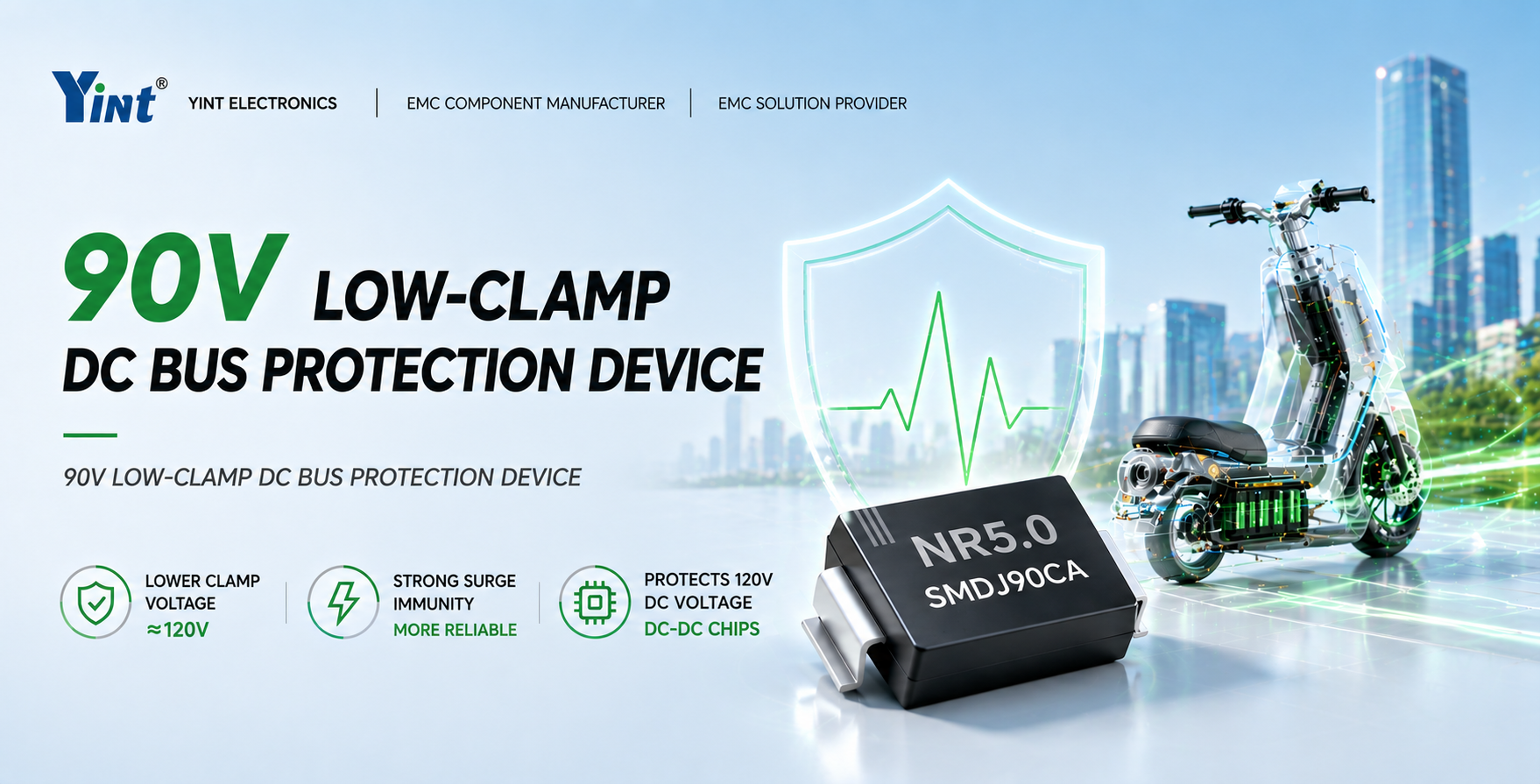
90V DC Bus Low-Clamping TVS Surge Protection Solution|120V Withstand DC
2026-05-14
NR5.0SMDJ90CA low clamping TVS diode protects 90V bus systems, clamping surges near 120V to prevent DC-DC chip breakdown and latent failure.
Explore More
Classification of the Core Framework for Global Regulation of Medical Devices
2025-08-24
China: Risk Classification System for Categories I, II, and III
According to the Medical Device Regulation (MDR 2017/745), the European Union classifies medical devices into Class I, Class IIa, Class IIb, and Class III, with risks gradually increasing
EMI Filter Fault Analysis and Solution Ideas
2025-08-23
1. What are possible reasons for severe heating of common mode inductors? How to troubleshoot?
Answer: Possible reasons:
Excessive differential mode current: Common mode inductors have weak suppression capability for differential mode current. If differential mode current in the circuit exceeds design values, it increases copper loss (I²R) in windings, causing heating.
Core saturation: When common mode current or differential mode current is too high, magnetic flux density in the core exceeds saturation point, permeability drops sharply, and eddy current losses increase dramatically, causing core heating.
· Abnormal winding resistance: Winding wires are too thin, local short circuits or poor contact during winding.
What is the area with the most frequent lightning activity in the world? Known as the 'Thunder City'
2025-08-22
What is the area with the most frequent lightning activity in the world? It is Lake Maracaibo in Venezuela Core data and phenomenon characteristics According to NASA's research, Lake Maracaibo experiences an average of 233 lightning strikes per square kilometer per year, far exceeding other regions. This data is 1.5 times that of the Congo Basin (recorded 158 square kilometers per year in Kifka village in 2004) and is also the "Lightning Capital" of Florida, United States; Orlando approximately 10 times per square kilometer per year
EMI Inductor Performance Testing and Verification Requirements Sharing
2025-08-20
1. What fixture should be used for insertion loss testing of common mode inductors? Why?
Answer: Insertion loss testing of common mode inductors typically uses 50Ω standard coaxial fixtures (such as BNC or SMA interface fixtures), and in some scenarios, they are used in conjunction with LINE IMPEDANCE STABILIZATION NETWORK (LISN). Reason: According to EMC testing standards (such as CISPR 16, IEC 61000-4-6), the characteristic impedance of the testing system needs to be unified to 50Ω.
10 Techniques for Using and Matching EMI Common Mode Inductors
2025-08-18
Question 1. How to optimize interference suppression above 10MHz through the combination of common mode inductors and Y capacitors?
Answer: Common mode inductors suppress interference through high common mode impedance from low to medium-high frequencies (e.g., below 1MHz), but at high frequencies (above 10MHz), impedance decreases due to parasitic capacitance (between windings, between windings and core), weakening suppression effect. Y capacitors (usually ceramic capacitors, such as MLCC) have low equivalent series resistance (ESR) and parasitic inductance (ESL), providing low impedance paths in high-frequency bands to divert common mode interference to ground. Optimization methods:
Capacitance selection:
EE! Times report: Trump's tariff fallacy: a homemade defeat
2025-08-17
The current US tariff strategy is based on a core fallacy that misjudges the complex reality of the global semiconductor industry. This self inflicted wrong policy did not lead the United States to victory, but instead resulted in strategic failure in its technological competition with China
EMI Inductor Installation and Layout Detail Matters
2025-08-15
1. What is the optimal distance between common mode inductors and X capacitors? Why?
Answer:
The optimal distance between common mode inductors and X capacitors is generally recommended to be controlled within 3-5cm. The reason is that common mode inductors mainly suppress common mode interference, while X capacitors mainly filter differential mode interference. The two need to work together to form an EMI filter.
If the distance is too far, parasitic inductance between leads increases, causing impedance matching of the filter network in high-frequency bands (e.g., above 100MHz) to be disrupted, and interference signals may "bypass" the filter through parasitic parameters...
Knowledge Points on EMI Inductor Application Scenarios Sharing
2025-08-14
1. What special parameter requirements do common mode inductors need to meet in 5G base station power supplies?
Answer:
High-frequency response and low parasitic capacitance: Need to maintain high impedance (e.g., above 1000Ω) in frequency bands above 100MHz, parasitic capacitance needs to be <10pF to avoid high-frequency signal leakage.
High saturation current: Meet large current requirements of base station power supplies (e.g., above 10A). Core materials preferably nanocrystalline or iron silicon aluminum to balance saturation characteristics and high-frequency loss.
Wide temperature range: Operating temperature needs to cover -40°C to +85°C, some outdoor base stations require...
Key Points on EMI Inductor Materials and Structure Selection Knowledge Sharing
2025-08-10
Point 1. What is the impedance difference between MnZn ferrite and NiZn ferrite common mode inductors at 30MHz frequency?
Answer: The permeability of MnZn ferrite can reach 5,000,
but permeability may start to decline at 20kHz frequency. At 30MHz frequency, its permeability has decreased significantly, resulting in relatively low impedance.
NiZn ferrite has low initial permeability but maintains permeability unchanged at high frequencies (100MHz). At 30MHz, it can maintain certain permeability, so impedance is relatively high. However, specific...
总计 444
1
2
...
17
18
19
20
21
22
23
...
49
50

 Global


 沪公网安备31011702889749号
